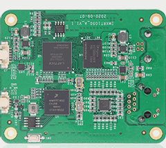
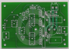
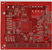
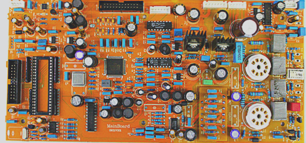
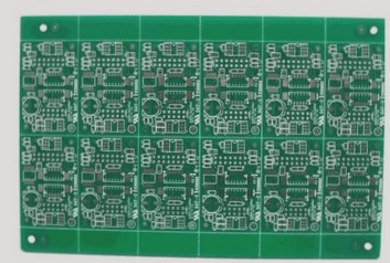
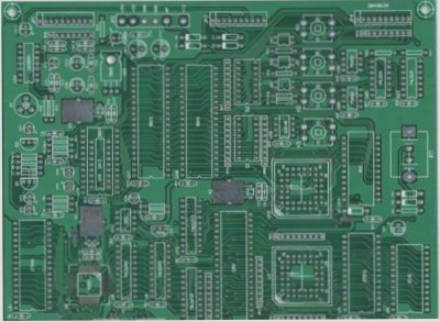
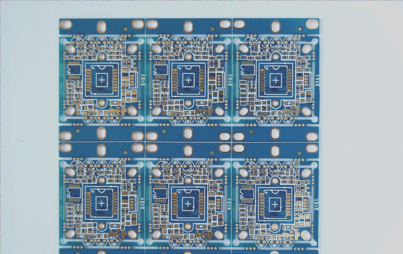
Ensure optimal PCB layout by minimizing signal trace lengths, placing parallel ground traces for traces longer than 300mm, minimizing loop area between signal lines and returns, alternating signal and ground trace positions every few centimeters for longer traces, centrally driving signals to multiple receivers, minimizing loop area between power and ground, positioning high-frequency capacitors near IC power pins, placing high-frequency bypass capacitors within 80mm of connectors, filling unused areas with ground planes, connecting ground fills across layers every 60mm, ensuring large ground fills are connected at both ends, using narrow traces for gaps exceeding 8mm on planes, keeping reset, interrupt, and edge-triggered signals away from PCB edges, connecting mounting holes to ground or isolating them, using zero-ohm resistors for metal bracket connections, determining mounting hole sizes for reliable bracket installation, using large pads on mounting holes and avoiding solder resist on bottom pads, avoiding parallel routing of protected and unprotected signals, paying special attention to routing reset, interrupt, and control signals, implementing high-frequency filtering, maintaining separation from I/O circuits, avoiding PCB edge placement for critical signals, inserting PCB proofing into enclosures rather than exposed positions, addressing wiring under magnetic beads to prevent unintended conductive paths, positioning static-sensitive PCBs centrally in multi-board housings, managing PCB etching differences between surfaces and edges, addressing colloidal buildup for uniform etching, and maintaining clean, functional etching equipment to prevent operational issues.


