PCB manufacturing process

PCB reverse engineering, circuit board layout, and schematic design

A PCB copy board involves reverse engineering a physical circuit board to recreate its design, including the schematic, layout, and components, enabling the exact replication of the original board.

PCB reverse engineering, circuit board layout, and schematic design Read More »

Subtractive Method for PCB Copy Board Design

The article explains the PCB subtractive manufacturing process, detailing the types of printed circuit boards produced (single-sided, non-plated through-hole, and plated through-hole), their respective production methods, and the advantages and disadvantages of the subtractive technique in PCB design and manufacturing.

Subtractive Method for PCB Copy Board Design Read More »

The function of PCB boards with different colors” can be rephrased in a more professional tone as: “The role of color variations in PCB boards

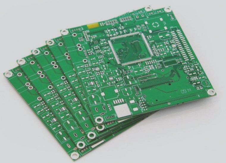
The color of PCB boards, often green due to its cost-effectiveness, visibility, and minimal eye strain, plays a role in the manufacturing process but does not necessarily indicate product quality, as other colors like black and blue are used for aesthetic or functional reasons.

The function of PCB boards with different colors” can be rephrased in a more professional tone as: “The role of color variations in PCB boards Read More »

Discussion on the V-Cutting Techniques for Circuit Boards

The V-cut technique in PCB manufacturing involves creating V-shaped grooves to facilitate the separation of circuit boards after SMT assembly, with precise control over depth being crucial to avoid damage or deformation.

Discussion on the V-Cutting Techniques for Circuit Boards Read More »

Manufacturing Process of an Eight-Layer Printed Circuit Board

The eight-layer PCB manufacturing process involves a complex, high-precision approach with multiple layers for signal and power planes, ensuring high performance and quality, while addressing challenges like copper foil creasing, film handling, and drilling techniques.

Manufacturing Process of an Eight-Layer Printed Circuit Board Read More »

Electrical Testing and Multi-layer PCB Manufacturing Process – 15 – PCB Fabrication Details – Wellcircuits

After all the manufacturing processes of the circuit board have been completed the electrical test is carried out to check the board for open circuits and short circuits The two most commonly used t

Electrical Testing and Multi-layer PCB Manufacturing Process – 15 – PCB Fabrication Details – Wellcircuits Read More »

Surface Finish and Multi-layer PCB Manufacturing Process – 13 – PCB Manufacturing Information – Wellcircuits

Bare copper of PCB is easily oxidized by moisture when exposed to air and the resulting oxide layer of copper has a great impact on the soldering which may lead to cold soldering and even cause the

Surface Finish and Multi-layer PCB Manufacturing Process – 13 – PCB Manufacturing Information – Wellcircuits Read More »

The Importance of Selecting the Right Solder Mask Ink – An Overview of PCB Fundamentals – Wellcircuits

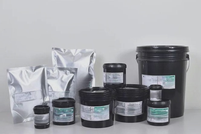
How Important is Solder Mask InkProvides insulation protectionActs as a safeguard against short circuits and corrosionEnhances the reliability and durability of the circuit boardEnsures stable tra

The Importance of Selecting the Right Solder Mask Ink – An Overview of PCB Fundamentals – Wellcircuits Read More »

Technology in the electroplating of PCB circuit boards

Modern PCB surface treatment technology combines traditional plating methods with advancements in materials science and engineering to enhance properties like conductivity, heat resistance, and wear resistance, while ensuring compatibility with substrate materials and the feasibility, controllability, and detectability of the coating process for high-quality, efficient manufacturing.

Technology in the electroplating of PCB circuit boards Read More »

Proficient in selecting the appropriate PCB via size based on design requirements.

This revised article explains the importance of vias in PCBs, their types (through, blind, and buried), and how to select appropriate parameters for drilling vias, while emphasizing the impact of manufacturing limitations on design decisions and the need for careful consultation with suppliers to ensure optimal performance and cost-efficiency.

Proficient in selecting the appropriate PCB via size based on design requirements. Read More »

Contact

WellCircuits
More than PCB

Upload your GerberFile(7z,rar,zip)