PCB pad

Types of PCB Pads: Essential PCB Knowledge and Basic Information – Wellcircuits

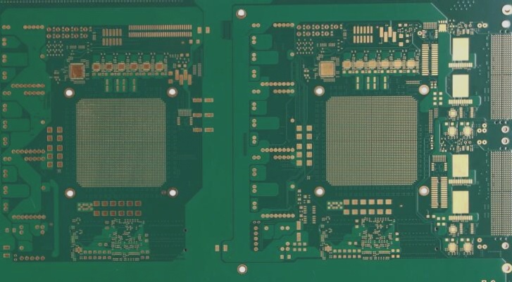
What is a PCB PadA pad is the exposed area of copper on a circuit board where the component lead is soldered The electrical connection of all components is made via pads The design and placement o

Types of PCB Pads: Essential PCB Knowledge and Basic Information – Wellcircuits Read More »

What are the precautions for the orientation and geometric design of printed circuit board (PCB) traces?

The precautions for the direction and shape of PCB printed wire include using short and simple wires, avoiding sharp bends or acute angles, maintaining equal distance between wires and pads, adjusting wire width based on pad spacing, reserving copper foil for common grounding wires, and providing a non-conductive production line on the PCB board to increase peeling strength of the pad.

What are the precautions for the orientation and geometric design of printed circuit board (PCB) traces? Read More »

Contact

WellCircuits
More than PCB

Upload your GerberFile(7z,rar,zip)