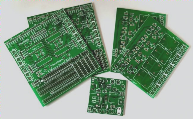
PCB processing

Process Specifications for PCB Fabrication

PCB processing requires a comprehensive understanding of various methods and materials, with strict adherence to procedures for handling, identification, and finishing to ensure high-quality, durable products while meeting environmental and industry standards.

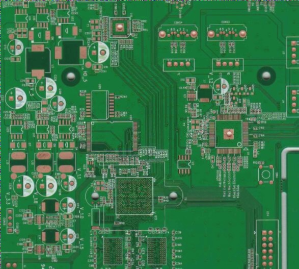
Process Specifications for PCB Fabrication Read More »

The aesthetic appearance of the green PCB substrate.

Green PCBs dominate the electronics industry due to their visibility during processing, environmental friendliness, and ease of inspection, despite no impact on performance, while various other colors are used primarily for differentiation.

The aesthetic appearance of the green PCB substrate. Read More »

Implement anti-static measures throughout the PCBA processing to ensure optimal performance.

PCB processing requires strict electrostatic protection measures due to the sensitivity of components, necessitating specific anti-static facilities, employee protocols, and operational guidelines to prevent electrostatic discharge.

Implement anti-static measures throughout the PCBA processing to ensure optimal performance. Read More »

What are the steps involved in the SMT placement machine processing?

SMT placement machines are essential in electronics manufacturing, involving a series of precise steps—screen printing, dispensing, placement, curing, reflow soldering, inspection, repair, and cleaning—to ensure high accuracy and efficiency in PCB assembly.

What are the steps involved in the SMT placement machine processing? Read More »

What are the consequences of inadequate plating in PCB patch processing?

To detect short circuits in PCB boards, use visual inspection, infrared imaging, and resistance testing with a digital multimeter, as well as consider board quality, since shorts can be hidden or cause burn marks in severe cases.

What are the consequences of inadequate plating in PCB patch processing? Read More »

Are you familiar with the PCB fabrication process?

The PCB processing flow involves cutting and preparing the copper substrate, applying and developing dry film photoresist for circuit patterns, pressing the inner and outer layers together, drilling for interlayer connections, plating through holes, and finally using photosensitive solder resist ink for better soldering performance.

Are you familiar with the PCB fabrication process? Read More »

Discussing the outer layer circuit etching process of the PCB.

The current PCB production primarily utilizes ammonia-based etchants for outer layer pattern etching, emphasizing uniform copper removal and minimal side etching despite challenges like residual accumulation affecting efficiency and quality.

Discussing the outer layer circuit etching process of the PCB. Read More »

PCB Industry’s Key Points

The PCB industry encompasses upstream raw materials, midstream manufacturing, and downstream applications across sectors like computer technology, communication, consumer electronics, and more, with PCBs serving as the structural foundation for electronic components and facilitating electrical connections among them.

PCB Industry’s Key Points Read More »

What are the factors leading to rosin joint formation during PCB processing?

Numerous factors contribute to rosin joints in PCB processing, including process issues, poor solderability, via holes, component pin distortion, and oxidation.

What are the factors leading to rosin joint formation during PCB processing? Read More »

Contact

WellCircuits
More than PCB

Upload your GerberFile(7z,rar,zip)