PCB testing

Electrical Testing and Multi-layer PCB Manufacturing Process – 15 – PCB Fabrication Details – Wellcircuits

After all the manufacturing processes of the circuit board have been completed the electrical test is carried out to check the board for open circuits and short circuits The two most commonly used t

Electrical Testing and Multi-layer PCB Manufacturing Process – 15 – PCB Fabrication Details – Wellcircuits Read More »

What is In-Circuit Testing (ICT) in PCB Assembly? – Wellcircuits

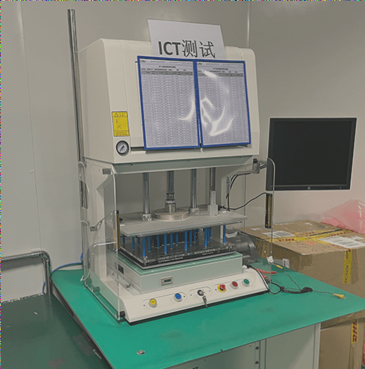
In-Circuit Testing ICT is a common method of testing electronic components and connections on a printed circuit board PCB to ensure that they are working correctly It is typically performed early

What is In-Circuit Testing (ICT) in PCB Assembly? – Wellcircuits Read More »

PCB Assembly Expertise and Skills in the Era of Industry 4.0

PCB testing is evolving in the Industry 4.0 era to integrate more rigorous and expansive testing methods, including enhanced evaluation of emerging features like system-on-chip designs, wireless protocols, and environmental resilience, to meet the demands of interconnected, high-performance PCBs.

PCB Assembly Expertise and Skills in the Era of Industry 4.0 Read More »

What is the function of AOI (Automated Optical Inspection) testing technology?

AOI (Automated Optical Inspection) is an advanced electronic testing technology used in PCB duplication, which helps detect defects during the production process by scanning PCBs and comparing them to predefined parameters, ensuring both end-product quality and process tracking across various stages such as solder paste printing, component placement, and reflow soldering.

What is the function of AOI (Automated Optical Inspection) testing technology? Read More »

The circuit board manufacturer explains the process of compound treatment.

The article discusses the evolution of testing fixtures for circuit boards, highlighting the shift from universal fixtures to dedicated and composite fixtures to meet the increasing demands of high-density surface mount designs, while also exploring the challenges and future prospects of testing methods, including non-contact technologies.

The circuit board manufacturer explains the process of compound treatment. Read More »

Standard Testing Methods for Printed Circuit Boards (DFT)

Preparing a test strategy for printed circuit boards involves understanding limitations related to accessibility, design size, function, and testing methods, and requires a comprehensive approach that considers various testing technologies and their associated benefits and drawbacks.

Standard Testing Methods for Printed Circuit Boards (DFT) Read More »

Comprehend the concept of In-Circuit Testing (ICT) for PCBA circuit boards.

Effective PCB product testing through ICT improves quality and profitability by detecting defects early in the electronics manufacturing process.

Comprehend the concept of In-Circuit Testing (ICT) for PCBA circuit boards. Read More »

Prototype of rigid PCB by Chinese PCB manufacturer

A rigid PCB prototype is a functional sample of a printed circuit board (PCB) created before manufacturing the final product. It serves a critical role in the PCB design process by enabling designers to test and verify their design’s functionality prior to mass production. Prototypes can be developed using methods such as breadboarding, solderless breadboarding, or PCB design software to create a virtual prototype. After creation, the prototype undergoes functional testing, allowing for necessary adjustments before moving to mass production. Rigid PCB prototypes are crucial for saving time and costs by identifying and rectifying design flaws early in the process. PCB manufacturing encompasses designing, fabricating, and assembling PCBs for electronic devices. The process typically involves these steps: Design: PCB manufacturing begins with designing the circuit board using specialized software to create a schematic and layout components and traces on the board. Fabrication: Once the design is complete, the PCB undergoes fabrication. This includes transferring the design onto a copper-clad board and etching to remove unnecessary copper. Drilling: After etching, the board is drilled to create holes for components and vias (connections between PCB layers). Plating: The board is then plated with a thin layer of copper to form conductive traces. Soldermask: A solder mask is applied to protect exposed copper and prevent solder bridges between traces. Silkscreen: A silk screen is applied to label components and indicate polarity on the board. Assembly: The final step involves manually or automatically assembling components onto the board. Overall, PCB manufacturing is a complex process requiring high expertise and precision to ensure the final product’s reliability and functionality.

Prototype of rigid PCB by Chinese PCB manufacturer Read More »

The PCB History & Vital Testing

A PCB, or printed circuit board, directs power through laminated copper sheets and, when enhanced with extra components, becomes a PCA (published circuit assembly) or PCBA (printed circuit board assembly). Proper PCB testing is crucial for quality control, as pioneered by Paul Eisler in 1936. Choosing reliable PCB services ensures high-quality products, saving money and enhancing company reputation through effective quality control measures.

The PCB History & Vital Testing Read More »

Contact

WellCircuits
More than PCB

Upload your GerberFile(7z,rar,zip)