pcb way

How does PCB laminate influence high-speed data transmission rates?

The article highlights that achieving high-speed data transmission on PCBs requires careful attention to laminate construction, as even minor changes can disrupt data paths and cause signal misalignment, affecting performance.

How does PCB laminate influence high-speed data transmission rates? Read More »

Defects in Reflow Soldering and BGA Package Circuits

Emergency methods for addressing BGA integrated circuit soldering issues include using solder paste to enhance solder ball adhesion, employing a hot air gun to heat the chip evenly, and applying moderate pressure to ensure proper contact between the solder balls and the PCB. These methods are crucial for effective repair under non-professional conditions.

Defects in Reflow Soldering and BGA Package Circuits Read More »

Here is the replacement spring for computer PCB circuit boards.

Following Snowden’s revelation of U.S. surveillance activities, China faces significant challenges and opportunities, particularly in advancing its computer sector through PCB copy board innovation to achieve IT localization and ensure information security.

Here is the replacement spring for computer PCB circuit boards. Read More »

Typical Issues in the Copper Sulfate Electroplating Process

Copper electroplating is essential for enhancing coating adhesion and protection in various applications, with common issues including rough plating, copper particles, pits, and uneven coloration, which can be addressed through process adjustments and quality control measures.

Typical Issues in the Copper Sulfate Electroplating Process Read More »

Various methods for managing plug holes in PCBs

As electronic products become lighter and more compact, PCB technology evolves towards higher density and complexity, leading to various methods for managing plug holes in PCBs, each with distinct processes, advantages, and challenges.

Various methods for managing plug holes in PCBs Read More »

Quality Assurance in PCBA and SMT Manufacturing Processes

Effective quality control in PCBA processing involves rigorous inspection and adherence to standards at every stage, from pre-production meetings and component procurement to SMT assembly and final testing, ensuring each step maintains high quality to prevent defects and failures.

Quality Assurance in PCBA and SMT Manufacturing Processes Read More »

Enhancing OSP Surface Treatment on PCBs: Improvement Strategies

1. Azole OSP is the preferred choice due to its high decomposition temperature and suitability for lead-free processes, crucial for selecting OSP type in PCB production. 2. OSP film thickness directly impacts solderability and thermal shock resistance; precise control is essential during PCB manufacturing. 3. OSP board production involves several critical steps: board placement, degreasing, washing, micro-etching, pre-soaking, application of OSP, and drying. 4. Key factors influencing OSP film thickness include degreasing effectiveness, micro-etching consistency, pre-soaking methods, OSP solution composition, pH control, temperature management, and dip coating time. 5. UV spectrometers or FIB technology are utilized for OSP film thickness measurement, ensuring adherence to industry standards. 6. Proper OSP board packaging and storage prevent film damage from humidity and temperature, crucial for maintaining solderability. 7. OSP boards require careful handling in SMT processes to avoid film damage, ensuring optimal solderability and component placement efficiency.

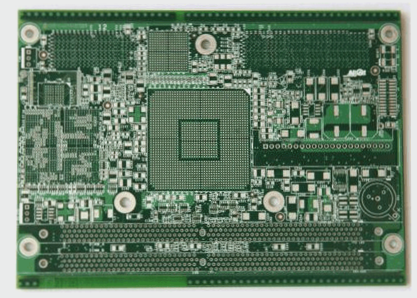
Enhancing OSP Surface Treatment on PCBs: Improvement Strategies Read More »

Definition and Description of the Twelve Levels of PCB Design

The PCB layers include top and bottom copper traces, solder mask layers, solder paste layers, screen printing layers, mechanical layers for shape representation, keepout layers for prohibited areas, midlayers for multi-layer boards, internal planes for electrical layers, through hole layers, drilling positioning layers, and drilling description layers.

Definition and Description of the Twelve Levels of PCB Design Read More »