penerangan ringkas jenis-jenis pcb

The company has opted to outsource the PCB design.

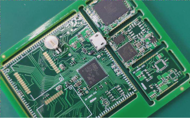
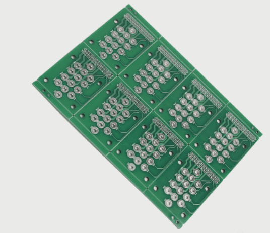
China’s PCB industry has grown rapidly, becoming the largest global producer, but faces challenges such as talent shortages, technological gaps, and an uneven distribution of applications, leading to a rising trend in outsourcing PCB design to specialized firms for enhanced efficiency and quality.

The company has opted to outsource the PCB design. Read More »

Comprehensive PCB Design Process

The process of designing a PCB schematic involves searching for existing components in the library or creating new ones if necessary, ensuring proper component pin configurations, running component rule checks, and following a structured workflow for accuracy and compliance with electrical standards.

Comprehensive PCB Design Process Read More »

Thermal Design Considerations and Characteristics of PCBA

The PCBA welding and heating process requires precise temperature control and thermal design to avoid soldering defects like tombstoning, BGA joint failure, and QFP pin openings, with key strategies including the use of heat sink pads and optimized reflow profiles to ensure uniform heat distribution and reliable connections.

Thermal Design Considerations and Characteristics of PCBA Read More »

The Impact of Humidity on PCBA Manufacturing Process

Humidity significantly affects PCBA manufacturing, with low humidity increasing electrostatic discharge and friction-related issues, while high humidity causes moisture absorption, leading to defects like delamination and poor soldering, making precise humidity control essential for ensuring production quality and reliability.

The Impact of Humidity on PCBA Manufacturing Process Read More »

Introduction to Three Types of Holes for PCB Prototyping

The text explains the different types of vias used in PCB manufacturing—through holes, blind holes, and buried vias—each serving distinct purposes in connecting circuit layers, with varying levels of complexity, cost, and space utilization.

Introduction to Three Types of Holes for PCB Prototyping Read More »

Could you provide an update on the condition of the patina on the PCB board?

The absence of conformal coatings on PCBs can lead to issues like patina formation, leakage, short circuits, and contamination from fingerprints or sweat, which can significantly shorten the product’s lifespan and increase maintenance costs.

Could you provide an update on the condition of the patina on the PCB board? Read More »

Advantages and Disadvantages of Three 3D Printing Technologies: FDM, SLA, and SLS – Wellcircuits

FDMAdvantages Easy to operate and maintainMore economical and cost-effective compared to other methodsNo need to use irritating chemicals which is more environmentally friendly Suitable size which c

Advantages and Disadvantages of Three 3D Printing Technologies: FDM, SLA, and SLS – Wellcircuits Read More »

What is a Fiducial Mark? – PCB Knowledge and Manufacturing Insights – Wellcircuits

What is a Fiducial Mark and How Does it WorkA fiducial mark is typically a circular pad or other shapes of exposed copper that is surrounded by a clearance area It acts as a reference point for auto

What is a Fiducial Mark? – PCB Knowledge and Manufacturing Insights – Wellcircuits Read More »

Contact

WellCircuits
More than PCB

Upload your GerberFile(7z,rar,zip)