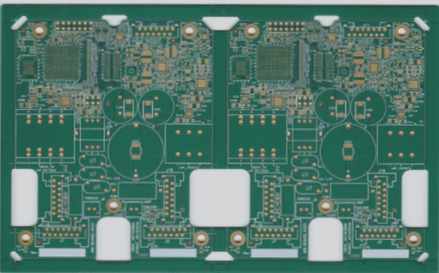
Optimizing the Balance of Power Supply Design in PCB
The design of a PCB’s power distribution network (PDN) requires careful consideration of trade-offs to minimize loop inductance, optimize capacitor placement, trace length, hole spacing, and dielectric thickness, thereby improving decoupling performance and reducing susceptibility to high-frequency noise.
Optimizing the Balance of Power Supply Design in PCB Read More »


