Minimizing Signal Coupling in RF Design
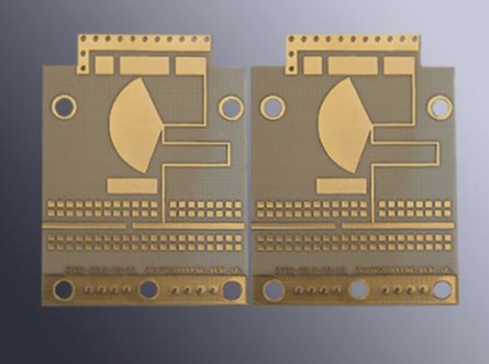
RF PCB board design is complex and challenging, with guidelines that must be carefully followed to accommodate various design constraints and overcome challenges such as integrating multiple functions in a compact space. Effective RF layout design involves isolating high-power and low-power circuits, implementing chip and power supply decoupling, and carefully placing components along the RF path to ensure signal integrity and minimize noise. Thorough planning and adherence to design principles are vital for successful RF layout design.

