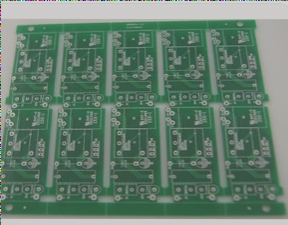
six-layer PCB

Why are six-layer PCBs commonly used?

A six-layer PCB features a stack of conductive layers with two inner signal layers, two outer signal layers, and dedicated power and ground planes, offering enhanced EMI suppression, improved routing for both low- and high-speed signals, and compact design ideal for high-frequency or high-speed applications.

Why are six-layer PCBs commonly used? Read More »

Investigate the applications of multi-layer PCB technology.

The design and advantages of multi-layer PCBs, specifically focusing on six-layer PCBs, which optimize performance by minimizing electromagnetic interference (EMI), enhancing signal routing, and providing high-density, compact, and reliable designs for both analog and digital circuits.

Investigate the applications of multi-layer PCB technology. Read More »

Contact

WellCircuits
More than PCB

Upload your GerberFile(7z,rar,zip)