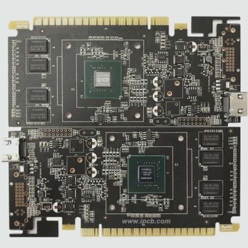
Analysis of Synchronous Switching Noise Generated by FPGA on PCB
Today’s CMOS technology allows a single FPGA device to have multiple I/O interfaces, and it is crucial for FPGA users to accurately measure and quantify system-level SSN on the PCB board. This article provides a comprehensive introduction to SSN, with a specific focus on SSN caused by FPGA output buffering, and presents several PCB board design techniques that can effectively reduce SSO.
Analysis of Synchronous Switching Noise Generated by FPGA on PCB Read More »

