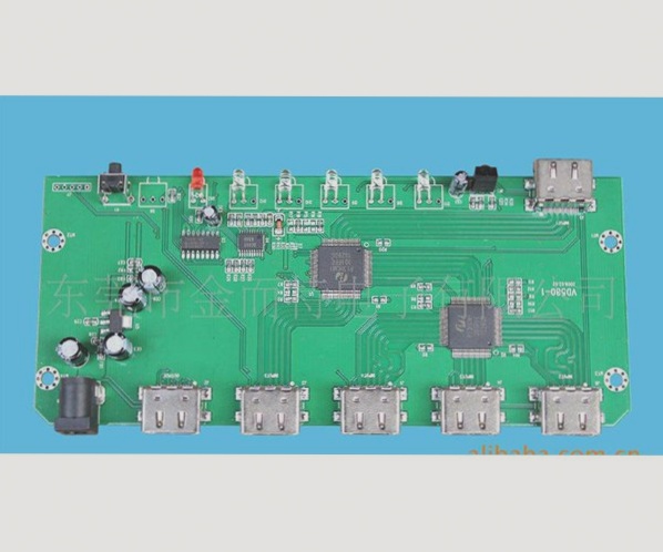
Utilizing filler blocks for pad design is a common misconception in PCB layout.
Understanding the complexities of PCB circuit board design is crucial, as issues like ambiguous processing levels, insufficient spacing, inadequate pad designs, and placement errors can lead to significant manufacturing challenges and functionality problems.
Utilizing filler blocks for pad design is a common misconception in PCB layout. Read More »

