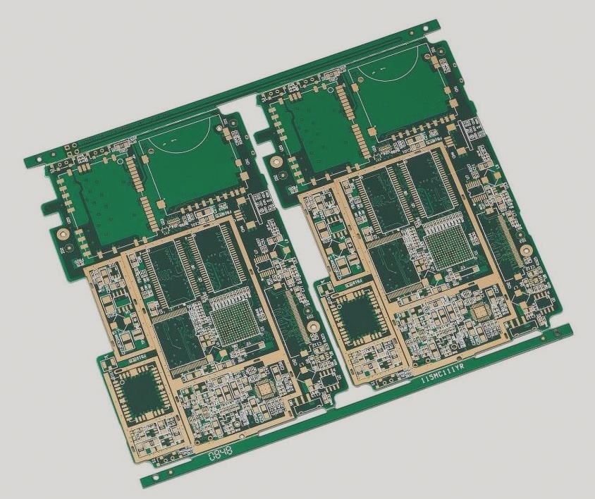
switching power supply design

PCB design for switching power supply circuits

The design of a switching power supply layout should closely follow its electrical design, focusing on efficient component placement, minimizing trace lengths, optimizing power and ground paths, and ensuring proper verification and output of Gerber files for production.

PCB design for switching power supply circuits Read More »

Switching power supply PCB design and layout

Summary: Optimize PCB layout for switching power supplies by minimizing pulse voltage path lengths, directly connecting key components like transformers and rectifier tubes, reducing loop areas, and strategically placing capacitors. Emphasize EMC performance through careful capacitor selection and placement, ensuring adequate spacing for heat dissipation and interference prevention in control circuits. Achieve high reliability by adhering to trace spacing guidelines, optimizing copper trace routing for current density, and selecting suitable board types based on application requirements and safety regulations.

Switching power supply PCB design and layout Read More »

Design specification for switching power supply PCB board

The physical design of the PCB board is crucial in any switching power supply design, as a poorly designed board can lead to excessive electromagnetic interference and unstable power supply operation. Key points to consider include parameter setting for trace spacing and pad design, proper placement of components, and careful layout of current loops to minimize interference. Adherence to designer rules and thorough outputting of design files is essential for a successful power supply design.

Design specification for switching power supply PCB board Read More »

Contact

WellCircuits
More than PCB

Upload your GerberFile(7z,rar,zip)