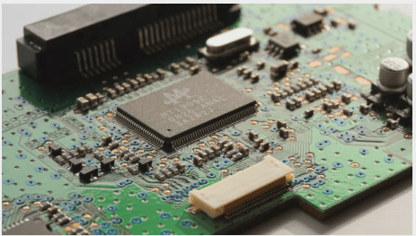
Key Considerations in the PCB Design Process
The PCB design process involves component parameter setup, schematic input, manual placement and routing, verification, review, and output, while emphasizing trace spacing, layout optimization, grounding, and careful design review to ensure electrical safety and performance, especially in high-frequency switching power supplies.