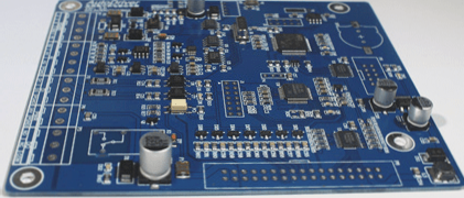
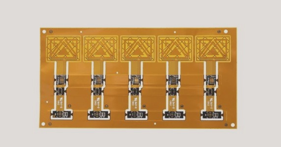
test points

Highly practical design for high-frequency PCB circuits

In high-speed PCB design, copper coating in blank areas is typically used for grounding, and the distribution between grounding and power supply should minimize impedance effects and signal integrity issues, with test point placement often requiring manual adjustments based on density and test specifications.

Highly practical design for high-frequency PCB circuits Read More »

Rationale for Incorporating Test Points in PCB Design

Adding test points to circuit board design facilitates comprehensive testing, ensuring soldering integrity and performance compliance post-PCBA completion, critical for identifying open or short circuits without compromising SMT component integrity, although challenges arise with needle bed testing on high-density boards, prompting consideration of alternative methods like JTAG, X-Ray, and AOI.

Rationale for Incorporating Test Points in PCB Design Read More »

Key considerations and best practices for setting test points on a PCB

Advancements in technology have led to shrinking circuit boards, creating challenges in accommodating numerous electronic components while maintaining adequate space for test points. Needle beds for circuit testing have inherent limitations, such as probe diameter constraints and spacing issues due to soldering requirements. Placement of needles near tall components can lead to collisions and damage, posing difficulties in accommodating test points for diverse components on PCBs. Discussions about reducing test points intensify as boards shrink, with alternative testing techniques emerging but not yet comprehensively replacing ICT. Manufacturers’ consultation regarding minimum test point diameter and distance constraints is crucial to ensure ICT needle implantation capabilities. Large-scale manufacturers may also impose constraints on the maximum distance between test points to prevent fixture damage.

Key considerations and best practices for setting test points on a PCB Read More »

The Importance of Test Points on PCB Boards

With the advancement of technology, the size of PCBs is shrinking, making it challenging to accommodate numerous electronic components. The issue of test points taking up valuable PCB space is a point of contention between design and manufacturing teams. Needle bed testing has limitations, such as minimum probe diameter and spacing restrictions, as well as risks of contact short circuits and potential damage to taller components. Alternative testing methods are emerging, but none can fully replace ICT testing. Consultation with fixture manufacturers is advised to ensure proper probe diameter and spacing for ICT needle implantation.

The Importance of Test Points on PCB Boards Read More »

Online PCB Test

PCB online testing detects manufacturing defects using needle fixtures, with an emphasis on setting testing touchpoints for defect analysis and performance consistency. Effective test plans include probe pads arranged on a grid and consideration of fault isolation, signal accessibility, and functional design considerations for efficient and accurate testing.

Online PCB Test Read More »

What is the importance of test points on FR4 PCBs?

Test points on FR4 PCBs are used to verify component specifications and solderability, preventing direct probe contact with electronic parts and enabling efficient testing with In-Circuit-Test (ICT) machines, but as circuit boards shrink in size, the battle between design and manufacturing and the limitations of using a needle bed for circuit testing remain ongoing challenges.

What is the importance of test points on FR4 PCBs? Read More »

Contact

WellCircuits
More than PCB

Upload your GerberFile(7z,rar,zip)