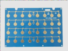
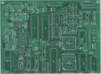
trace spacing

What safety clearance issues might arise in PCB design?

In PCB design, safety spacing concerns can be categorized into electrical and non-electrical safety distances, with key considerations including trace spacing, pad-to-pad distance, copper edge clearance, silk screen placement, and component compatibility with the mechanical structure.

What safety clearance issues might arise in PCB design? Read More »

18 Advanced Layout Techniques for PCB Circuit Boards

Effective PCB layout is crucial for reliability and performance, and following guidelines like maintaining trace spacing, balancing copper, minimizing EMI, avoiding sharp angles, and ensuring proper heat dissipation can prevent costly issues and board failures.

18 Advanced Layout Techniques for PCB Circuit Boards Read More »

PCB Wiring and Layout for Advanced Technological Expansion

To minimize interference and optimize PCB design, increase trace spacing, route lines at right angles, classify and separate wiring, place components close to power supplies, and manage impedance, capacitance, and inductance effectively.

PCB Wiring and Layout for Advanced Technological Expansion Read More »

Contact

WellCircuits
More than PCB

Upload your GerberFile(7z,rar,zip)