via design

Fundamentals of PCB Design and Circuit Board Engineering

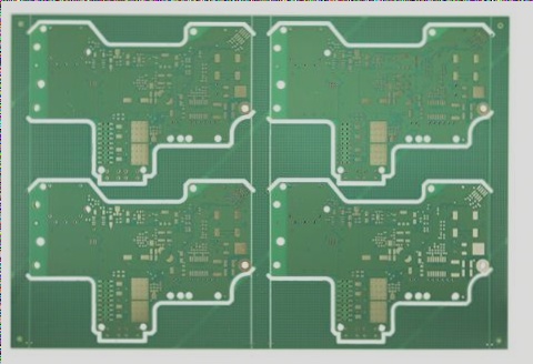
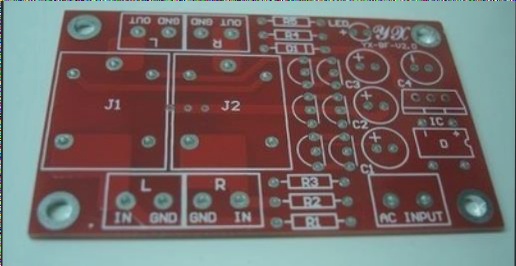
The “layers” in PCB design refer to the actual physical copper layers of a circuit board, with modern designs often including multiple layers for routing and power distribution, while concepts like vias, silk screen, SMD components, and fill areas must be carefully managed to ensure a functional and manufacturable design.

Fundamentals of PCB Design and Circuit Board Engineering Read More »

Are you familiar with via design considerations in high-speed PCBs?

In high-speed PCB design, vias are crucial for interlayer connections, but their parasitic capacitance and inductance can significantly affect signal integrity at frequencies above 1 GHz, making careful via design essential to minimize these negative impacts.

Are you familiar with via design considerations in high-speed PCBs? Read More »

Six Commonly Utilized Via Processing Methods in PCB Design

Vias are essential in multi-layer PCBs, with drilling costs making up a significant portion of PCB manufacturing costs. Designers aim for smaller via sizes for high-speed circuits, but must consider limitations in drilling and plating processes. It is recommended to follow specific guidelines for via sizes and placements to ensure optimal performance and avoid production issues.

Six Commonly Utilized Via Processing Methods in PCB Design Read More »

Contact

WellCircuits
More than PCB

Upload your GerberFile(7z,rar,zip)