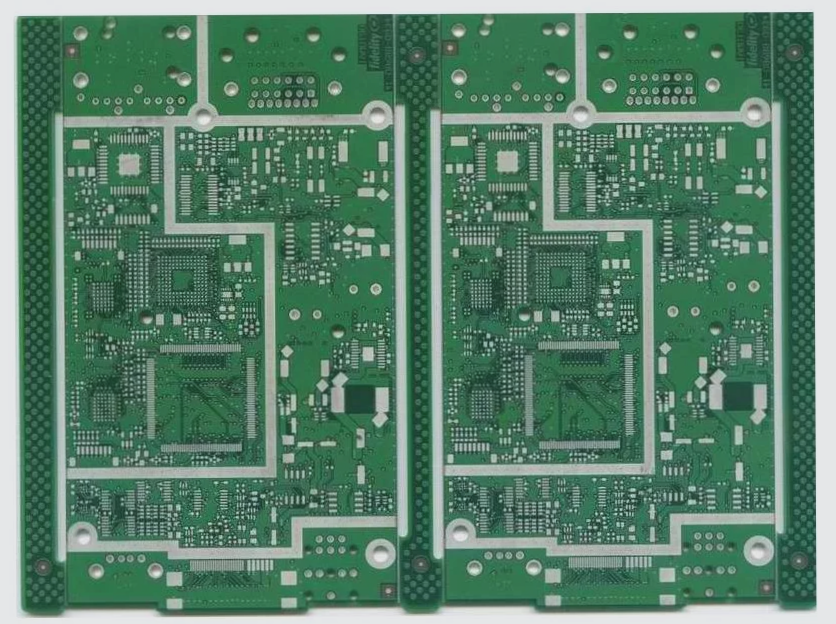
How can one ascertain the number of layers required for a PCB design?
To determine the number of layers in a PCB, observe the via holes and light transmission: if vias are visible on both sides, it’s likely a 4-layer board; if vias are visible only on one side or light passes through them, it could be a 6/8-layer board; multilayer boards with opaque inner cores may have many more layers.
How can one ascertain the number of layers required for a PCB design? Read More »