Wave Soldering

Analysis of Challenges in the Selective Soldering Process of PCBs

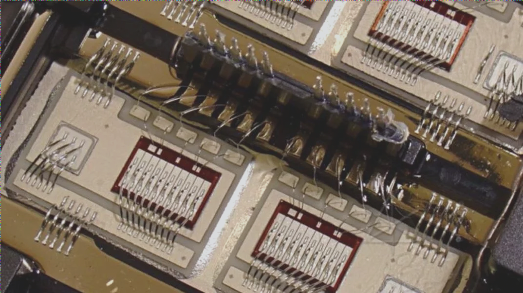
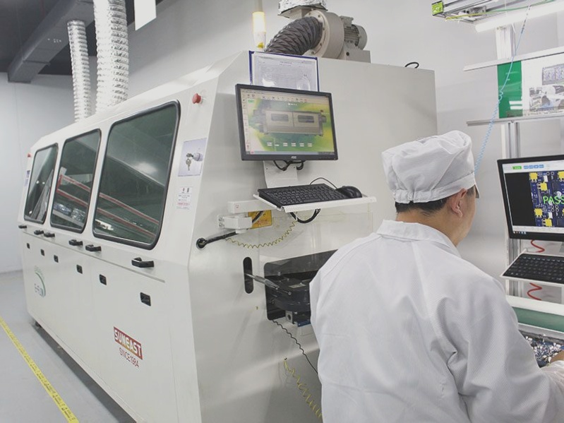
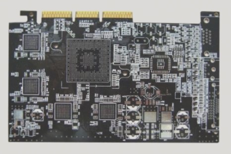
1. Selective soldering in the PCB electronics industry offers advantages over traditional wave soldering by focusing solder application on specific areas, reducing costs, and accommodating sensitive components, thereby driving its increased adoption.

Analysis of Challenges in the Selective Soldering Process of PCBs Read More »

Optimize Component Layout: 17 Requirements for Flawless SMT Process

Component layout in PCB design should adhere to SMT electronic processing requirements, considering distinct processes like reflow soldering and wave soldering, aiming for uniformity, heat dissipation, and ease of access, while minimizing soldering defects and damage risks.

Optimize Component Layout: 17 Requirements for Flawless SMT Process Read More »

Intro to PCB Selective Welding Tech

In recent electronics industry trends, reflow soldering is prominent, but challenges with temperature-sensitive elements have led to a shift towards selective soldering, offering efficient, economical soldering for remaining cartridge components while ensuring compatibility with lead-free requirements.

Intro to PCB Selective Welding Tech Read More »

Introduction to Wave Soldering and Reflow Soldering Sequence

Wave soldering and reflow soldering are two different methods used in electronic manufacturing to create mechanical and electrical connections between components and circuit boards, with each method being suitable for different sizes of components.

Introduction to Wave Soldering and Reflow Soldering Sequence Read More »

Guide to Wave Soldering Avoidance

Tin appearance on PCB boards post-wave soldering may arise from various factors beyond just design flaws. Issues like inadequate flux activity, uneven application, or uncontrolled solder temperature can contribute. While not all issues stem from design, designers must ensure correctness. To mitigate tin formation, focus on flux activity, wettability, and solder temperature during wave soldering.

Guide to Wave Soldering Avoidance Read More »

Optimizing Wave Soldering Processes for PCBA Packaging

The initial stage of wave soldering in PCBA packaging is crucial for quality control, involving steps such as pre-drying to prevent PCB warpage, adjusting preheating temperature for optimal solder fluidity, and determining transmission speed and angle to ensure even soldering.

Optimizing Wave Soldering Processes for PCBA Packaging Read More »

What are the distinctions between DIP wave soldering and reflow soldering in PCB assembly processes?

Welding is critical in PCB design, with wave soldering and reflow soldering being common techniques, each suitable for different scenarios. Wave soldering is used for through-hole components, while reflow soldering is preferred for surface mount components. WellCircuits specializes in PCBA manufacturing, providing reliable electronic assembly services across multiple industries.

What are the distinctions between DIP wave soldering and reflow soldering in PCB assembly processes? Read More »

Contact

WellCircuits
More than PCB

Upload your GerberFile(7z,rar,zip)