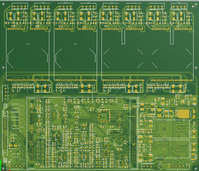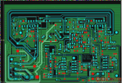
Technique for Segregating Electrical Layers within a PCB
To divide an inner electric layer of a multilayer PCB, define the layer, use the “Split Planes” command to set segmentation, adjust track width for insulation, select networks, and draw boundaries while avoiding overlap with pads to ensure proper connectivity and minimize impedance.
Technique for Segregating Electrical Layers within a PCB Read More »