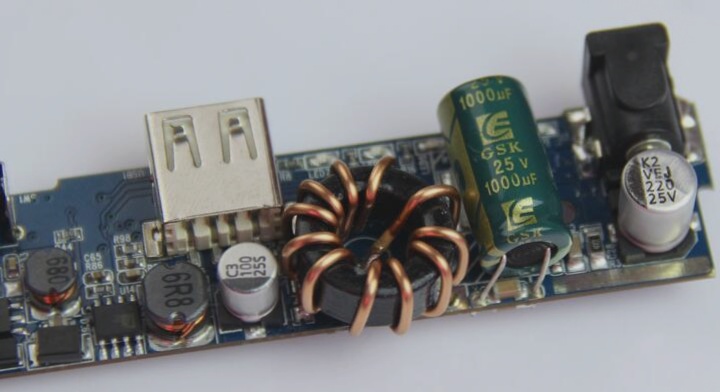
Arrangement of traces and components on the printed circuit board
The design process for printed circuit boards (PCBs) involves strategically placing components, ensuring proper spacing and isolation for high and low voltage circuits, optimizing wire routing, and implementing effective grounding and shielding to enhance performance and minimize interference.
Arrangement of traces and components on the printed circuit board Read More »

