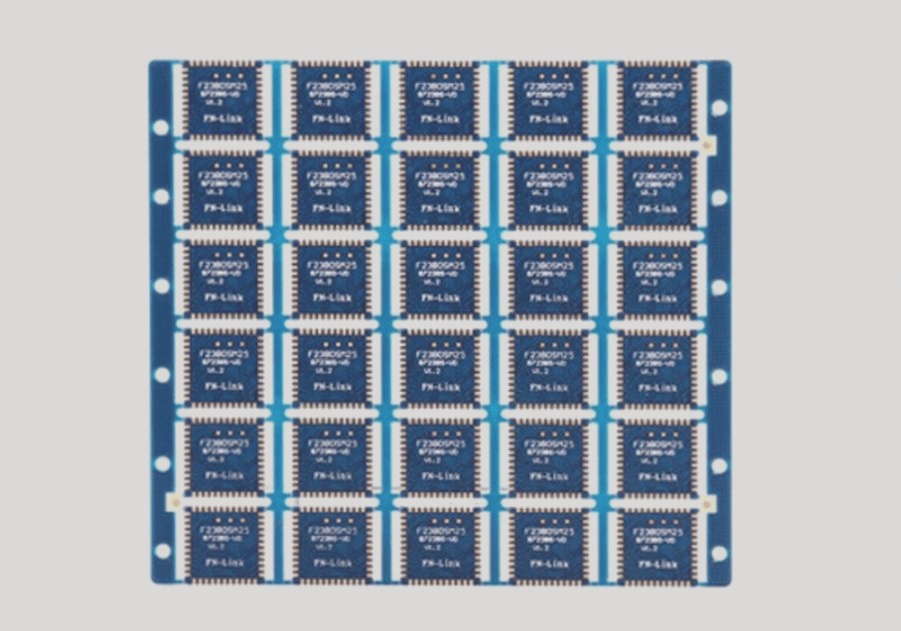
For electronic equipment, some heat is generated during operation, causing the internal temperature to rise rapidly. If this heat is not dissipated promptly, the equipment will continue to overheat, leading to device failure and a decline in reliability.
Thus, effective heat management of the circuit board is crucial. The heat dissipation of a PCB is a vital aspect of its design. What techniques can be employed for effective heat dissipation in PCBs? Let’s explore this together.
**One**
Heat is dissipated through the PCB itself. Currently, the most commonly used PCB substrates are copper-clad epoxy glass cloth and phenolic resin glass cloth, with a limited use of paper-based copper-clad boards.
While these substrates exhibit excellent electrical and processing properties, their heat dissipation capabilities are lacking. Given that high-power components generate heat, relying solely on the PCB resin for thermal conduction is nearly impossible; instead, heat must be transferred from the component surfaces to the surrounding air.
However, as electronic products have advanced towards miniaturization, high-density installations, and high-heat assemblies, relying solely on surface heat dissipation is inadequate due to the small surface area of many components.
Additionally, with the widespread use of surface-mounted components like QFPs and BGAs, a significant amount of heat produced by these components is transferred to the PCB. Therefore, an optimal solution for heat dissipation involves enhancing the thermal management capabilities of the PCB in direct contact with heat-generating elements, allowing for effective heat transmission or emission through the board.
This can be achieved by adding heat dissipation copper foil and enlarging the area of power supply copper foil. Utilizing thermal vias and exposing copper on the back of ICs can also help reduce thermal resistance between the copper layer and air.
**PCB Layout**
a. The thermal sensing device should be positioned in the cooler air zone.
b. The temperature detection device should be placed in the hottest location.
c. Devices on the same printed board should be organized into zones based on their heat generation and dissipation characteristics. Low heat-generating devices or those with poor heat resistance (e.g., small signal transistors, small-scale integrated circuits, electrolytic capacitors) should be located at the inlet of the cooling air flow, while high heat-generating devices or those with good heat resistance (e.g., power transistors, large-scale integrated circuits) should be positioned downstream in the air stream.
d. Horizontally, high-power devices should be placed as close to the edge of the printed board as possible to minimize the heat transfer distance; vertically, they should be positioned near the top of the board to lessen their impact on the temperature of other components.
e. The heat dissipation of printed boards largely relies on airflow, so the airflow path must be considered in the design. Devices or printed circuit boards should be arranged thoughtfully. Air naturally flows to areas of lower resistance, so it’s essential to avoid large air gaps in any specific area on the printed circuit board. This consideration also applies to the layout of multiple boards in the entire system.
f. The temperature-sensitive device should be placed in the coolest area (e.g., at the bottom of the equipment). It should never be positioned directly above any heating device. Devices should be staggered on the horizontal plane.
g. High-power and high-heat-generating devices should be located near effective heat dissipation areas. Avoid placing high-heat devices at the corners or edges of the printed board unless accompanied by a heat sink. When designing power resistors, opt for larger devices where feasible, ensuring adequate heat dissipation space during the layout process.
h. **Component Spacing Recommendations:**
High-heat devices should include heat sinks or thermal conduction boards. For a few high-heat components (fewer than three), a heat sink or thermal pipe can be added. If temperatures remain high, a heat sink with a fan may be utilized for improved dissipation. For larger quantities of heating components (more than three), a customized large heat dissipation cover can be employed, tailored to the positioning and height of the heating elements. This cover should contact each element directly for efficient heat transfer, often enhanced by adding a soft thermal phase change conduction pad on component surfaces to boost dissipation effectiveness.
i. For equipment relying on free convection cooling, it’s preferable to arrange integrated circuits (or other devices) longitudinally or transversely.
j. A reasonable wiring design should facilitate heat dissipation. Given that the resin in the board has low thermal conductivity, and copper foil lines and holes are excellent heat conductors, increasing the residual copper foil rate and adding heat conduction holes are primary methods for enhancing heat dissipation.
k. To assess the heat dissipation capability of a PCB, it’s essential to calculate the equivalent thermal conductivity (EQ) of the insulating substrate, which is a composite material with varying thermal conductivities.
l. Devices on the same printed board should be organized into zones based on their calorific values and heat dissipation levels. Low heat-generating devices should be positioned at the cooling air inlet, while high heat-generating devices should be located downstream.
m. In the horizontal layout, high-power devices should be as close to the board’s edge as possible to reduce the heat transfer distance; vertically, they should be near the top to mitigate their effect on other devices’ temperatures.
n. The heat dissipation of printed boards primarily depends on airflow, so the airflow path should be thoughtfully analyzed during design, ensuring reasonable device or PCB configurations. It’s crucial to avoid large air gaps in specific areas and maintain awareness of the same issue across multiple printed circuit boards in the overall machine.
o. Temperature-sensitive devices should be placed in the lowest temperature zones (e.g., at the bottom of the equipment) and should never be positioned directly above heat sources. Devices should be staggered horizontally to optimize cooling.
p. High-power consumption devices and significant heat-generating components should be arranged near effective heat dissipation zones. Avoid placing heat-intensive devices at the corners or edges of the printed board unless a heat sink is nearby. When designing power resistors, select larger devices whenever possible, ensuring sufficient space for heat dissipation in the layout.
q. Aim to avoid clustering hot spots on the PCB, distributing power evenly across the surface to maintain uniform temperature performance. Achieving perfect uniformity can be challenging, but it’s critical to avoid areas with excessive power density that could lead to hot spots affecting circuit operation. If feasible, analyzing the thermal efficiency of printed circuits is advisable. For instance, thermal efficiency analysis software integrated into some PCB design tools can aid designers in optimizing circuit layouts.