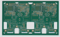
Double-Sided PCB Printed Circuit Boards: A Closer Look
- Our common computer boards are essentially double-sided PCBs made from epoxy glass cloth.
- One side is for component insertion, while the other is for soldering component pins.
- The solder joints are uniform, showcasing precision.
- The discrete soldering surface for component pins is known as a pad.
- Besides solder pads, other copper patterns aren’t tinned; they are covered with a solder mask to withstand wave soldering.
The Role of Solder Mask in PCBs
- Solder masks, predominantly green but also available in yellow, black, and blue, are crucial in preventing bridging during wave soldering.
- They enhance soldering quality, conserve solder, and act as a protective layer against moisture, corrosion, and mechanical wear.
- The smooth and glossy green solder mask improves aesthetics and increases the reliability of solder joints.
Evolution of Component Installation Methods
- Three methods for component installation are evident: plug-in installation, surface mounting, and direct chip mounting.
- Surface mount technology offers advantages such as increased wiring density, reduced board area, and improved product quality and reliability.
- Advancements in surface mounting technology are closely tied to improvements in circuit board technology and chip packaging.
Future Trends in PCB Production
- As PCB density rises, new technologies like laser technology and photosensitive resins are integrated into production processes.
- Technological advancements continue to drive the evolution of circuit board production, with areas like blind and buried vias, flexible boards, and photolithography expanding.
Explore the intricate world of PCBs and stay updated on the latest trends in circuit board technology!