The sensitivity of electronic equipment is continuously increasing, which requires these devices to have enhanced anti-interference capabilities. As a result, PCB design has become more challenging. Improving the anti-interference performance of PCBs has become a critical concern for many engineers. This article presents several strategies for reducing noise and electromagnetic interference (EMI) in PCB design.
Below are 24 tips to minimize noise and electromagnetic interference in PCB design, compiled from years of experience:
(1) Use low-speed chips where possible, reserving high-speed chips for critical areas.
(2) A series resistor can be added to reduce the rise and fall rates of the control circuit edges.
(3) Provide some form of damping for components such as relays to minimize noise.
(4) Choose the lowest frequency clock that meets the system’s requirements.
(5) Position the clock generator as close as possible to the device that uses the clock. The casing of the quartz crystal oscillator should be grounded.
(6) Surround the clock area with a ground plane and keep clock traces as short as possible.
(8) The unused end of the MCD should be connected to a high voltage, grounded, or defined as an output. Additionally, the power supply ground pin of integrated circuits should be properly connected, not left floating.
(9) Never leave unused gate circuit inputs unconnected. The positive input of an unused operational amplifier should be grounded, while the negative input should be connected to the output.
(10) When designing PCBs, use 45-degree angle traces instead of 90-degree angles to reduce high-frequency signal radiation and coupling.

(11) The printed circuit board (PCB) should be divided based on the frequency and current switching characteristics, with noise-sensitive and non-noise-sensitive components placed as far apart as possible.
(12) For single-sided and double-sided PCBs, a single-point power supply and single-point grounding should be used. The power and ground traces should be as wide as possible. If cost permits, consider using a multilayer board to minimize the capacitive and inductive effects of the power and ground planes.
(13) The clock, bus, and chip select signals should be kept away from I/O lines and connectors to minimize interference.
(14) The analog voltage input traces and reference voltage pins should be positioned as far away as possible from the digital signal traces, especially the clock signals.
(15) For A/D converters, it is better to keep the digital and analog sections integrated rather than having them cross over each other.
(16) A clock trace running perpendicular to I/O lines experiences less interference than one running parallel to them. Additionally, the clock pins of components should be kept away from the I/O traces.
(17) Component leads should be as short as possible, and the leads of decoupling capacitors should be especially short.
(18) Critical signal traces should be as wide as possible, with protective ground planes on both sides. High-speed traces should be kept short and as straight as possible.
(19) Noise-sensitive traces should not run parallel to high-current or high-speed switching lines to avoid interference.
(20) Avoid routing traces under quartz crystals or noise-sensitive components to reduce the risk of signal interference.
(21) For weak signal circuits, ensure that no current loops are formed around low-frequency circuits to prevent unwanted signal coupling.
(22) Never form loops in signal traces. If unavoidable, minimize the loop area as much as possible.
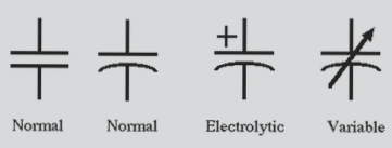
(23) Place one decoupling capacitor for each integrated circuit, and always add a small high-frequency bypass capacitor in parallel with each electrolytic capacitor.
(24) In PCB design, replace electrolytic capacitors with large-capacity tantalum or ceramic capacitors for energy storage in circuit charging and discharging applications. When using tubular capacitors, make sure the casing is grounded.
If your have any questions about PCB ,please contact me info@wellcircuits.com


