Effective Methods for EMI Suppression in PCB Design
- EMI suppression coatings, appropriate part selection, and simulation design are key modern methods for solving EMI issues.
- Power bus optimization: Placing capacitors near IC power supply pins improves voltage response, but more measures are needed for full-band harmonic power.
- Role of Power Layer: The power layer surrounding ICs acts as a high-frequency capacitor, reducing common-mode EMI and providing clean high-frequency output.
- Layer Stacking Techniques: Proper layering, inter-layer materials, and operational frequency are crucial for managing EMI effectively.
- Signal Trace Strategy: Consolidating signal traces onto layers adjacent to power or ground layers helps in EMI control.
For detailed PCB layer stacking examples and strategies, visit PCB Fabrication.

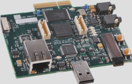
4-Layer PCB Challenges
Traditional 4-layer board designs may face issues due to excessive thickness between power and ground layers.
Optimizing PCB Design for EMI Control
To meet cost requirements initially, consider two alternative designs for traditional 4-layer boards. These solutions can enhance electromagnetic interference (EMI) suppression performance but are only suitable for low-component-density applications with ample area around components for required power copper layers.
- The preferred solution involves all outer PCB layers serving as ground layers, with the middle two layers dedicated to signals and power. Routing power supply on the signal layer with wide lines reduces power supply current path impedance and ensures low impedance for signal microstrip paths. This represents the optimal 4-layer PCB structure for EMI control.
- In the second scheme, outer layers serve as power and ground, with the middle two layers as signal layers. Though an improvement over traditional 4-layer boards, this scheme suffers from interlayer impedance issues similar to traditional designs. Careful placement of traces beneath power and ground copper islands is essential for impedance control, along with maximizing interconnection of copper islands to ensure DC and low-frequency connectivity.
6-Layer PCB Design
For higher component density than a 4-layer board, a 6-layer board is preferable. However, some stacking schemes in 6-layer board designs may inadequately shield electromagnetic fields and have minimal impact on transient signal reduction in power bus.
10-Layer PCB Design
Due to thin insulation layers between multilayer boards, impedance among the 10 or 12 layers is very low. Achieving excellent signal integrity is feasible provided proper layering and stacking. Manufacturing 12-layer boards at 62 mil thickness is challenging, with few manufacturers capable of processing such boards.
In the absence of closely located via holes, increased inductance and reduced capacitance are inevitable, leading to heightened EMI. When signal lines must traverse PCB wiring layers via vias, ground vias should be positioned near vias to facilitate smooth signal return to appropriate grounding layers. Signal loops on layers 4 and 7, for instance, return via power or ground layers (layers 5 or 6) where capacitive coupling between power and ground layers is optimal, enabling efficient signal transmission.