Is there a specific area of PCBA bonding strength you’re most interested in improving?
Is there any way to enhance the bonding force of PCBA?
Certainly, it largely depends on your budget for the solution. If you’re aiming to boost the bonding strength of PCBA, several avenues can be explored, such as “improving solderability,” which many R&D professionals favor, or investing in enhancing the bending resistance of FR4 boards. However, each method has its own advantages and disadvantages; otherwise, issues like solder cracking and component detachment wouldn’t continually challenge the electronics industry.
Methods to enhance the bonding force of PCBA solder: utilize copper base for surface treatment.
The advantages, drawbacks, and precautions associated with these methods for increasing the bonding force of PCBA will be discussed in detail below:
1. Switch to a “copper” base for PCB surface treatment.
Various PCB surface treatments and solder pastes lead to different solder intermetallic compound (IMC) formations, which in turn affect soldering strength. Since the primary component of solder paste is “tin,” the PCBs currently mass-produced in the industry are generally categorized into two types of surface treatment: “copper” base and “nickel” base.

1. ENIG (Electroless Nickel Immersion Gold) represents a “nickel” base. After soldering, it forms an intermetallic compound (IMC) of Ni3Sn4 when combined with “tin.” OSP, HASL, and ImSn are all “copper” bases, where “Sn” combines to create Cu6Sn5 IMC.
2. Generally, the bonding strength of Cu6Sn5 is superior to that of Ni3Sn4. This means the IMC formed by the copper base and solder paste is typically stronger than that of the nickel base. Hence, Shenzhen Honglijie has shifted its PCB surface treatment to copper base processes to enhance solder strength. Over time, the copper-based IMC may gradually transition to the less desirable IMC Cu3Sn, resulting in a relatively brittle and weaker solder strength, although this transformation may take several years. Additionally, all IMC layers will thicken over time, with high temperatures accelerating their growth rate.
3. I mentioned earlier that as the IMC thickens, its strength can diminish, but this deterioration is a long-term issue. It’s crucial to monitor IMC transformation and thickening when a long-term usage period or military standards are involved.
4. There is also the silver immersion board (ImAg), initially used with the lead-free process. However, due to numerous quality issues, particular care must be taken to avoid “sulfur” and “sulfide” contamination. Very few utilize this process, so I won’t delve into it further.
5. The ENIG surface treatment carries another potential risk: black nickel or black pad issues, which can significantly impair soldering quality.
6. Therefore, if a PCB company opts for ENIG boards, they should consider alternatives like OSP (Organic Protective Film), HASL (Hot Air Solder Leveling), or ImSn (Immersion Tin). It’s essential to note that boards with different surface treatments have varying shelf lives. Some treatments may require stringent compliance with reflow oven timings and processes, as the soldering outcomes can differ based on these factors, necessitating careful selection.
7. Not all companies can transition to using “copper” base boards, as they must assess their industry-specific characteristics. For instance, Shenzhen Honglijie faces challenges due to long product life cycles, often leading to small orders with unpredictable forecasts that may be modified post-placement, with PCB delivery typically taking 6 to 8 days. Sudden changes can hinder complete consumption of delivered boards during SMT, making longer shelf life, like that of ENIG, preferable for maintaining welding capabilities after repeated baking and dehumidification.
8. We avoid using OSP and similar boards entirely. To enhance BGA soldering capabilities, R&D specifically utilized a “selective OSP” board—applying OSP only in the BGA area while using ENIG elsewhere. However, many boards ultimately reverted to ENIG due to compliance and performance considerations.
Is there any way to enhance the bonding force of PCBA?
Certainly, it largely depends on your budget for the solution. If you’re aiming to boost the bonding strength of PCBA, several avenues can be explored, such as “improving solderability,” which many R&D professionals favor, or investing in enhancing the bending resistance of FR4 boards. However, each method has its own advantages and disadvantages; otherwise, issues like solder cracking and component detachment wouldn’t continually challenge the electronics industry.
Methods to enhance the bonding force of PCBA solder: utilize copper base for surface treatment.
The advantages, drawbacks, and precautions associated with these methods for increasing the bonding force of PCBA will be discussed in detail below:
1. Switch to a “copper” base for PCB surface treatment.
Various PCB surface treatments and solder pastes lead to different solder intermetallic compound (IMC) formations, which in turn affect soldering strength. Since the primary component of solder paste is “tin,” the PCBs currently mass-produced in the industry are generally categorized into two types of surface treatment: “copper” base and “nickel” base.
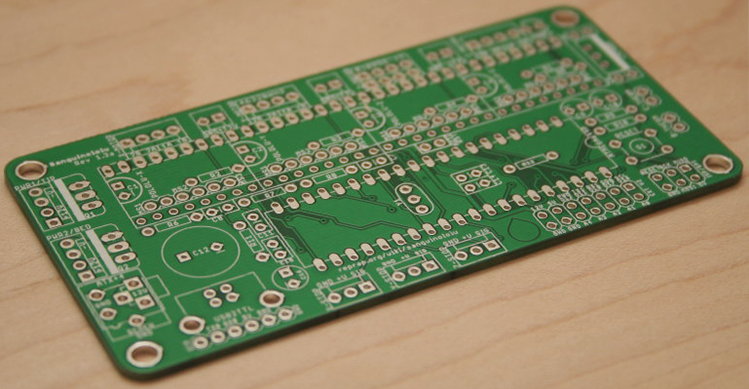
1. ENIG (Electroless Nickel Immersion Gold) represents a “nickel” base. After soldering, it forms an intermetallic compound (IMC) of Ni3Sn4 when combined with “tin.” OSP, HASL, and ImSn are all “copper” bases, where “Sn” combines to create Cu6Sn5 IMC.
2. Generally, the bonding strength of Cu6Sn5 is superior to that of Ni3Sn4. This means the IMC formed by the copper base and solder paste is typically stronger than that of the nickel base. Hence, Shenzhen Honglijie has shifted its PCB surface treatment to copper base processes to enhance solder strength. Over time, the copper-based IMC may gradually transition to the less desirable IMC Cu3Sn, resulting in a relatively brittle and weaker solder strength, although this transformation may take several years. Additionally, all IMC layers will thicken over time, with high temperatures accelerating their growth rate.
3. I mentioned earlier that as the IMC thickens, its strength can diminish, but this deterioration is a long-term issue. It’s crucial to monitor IMC transformation and thickening when a long-term usage period or military standards are involved.
4. There is also the silver immersion board (ImAg), initially used with the lead-free process. However, due to numerous quality issues, particular care must be taken to avoid “sulfur” and “sulfide” contamination. Very few utilize this process, so I won’t delve into it further.
5. The ENIG surface treatment carries another potential risk: black nickel or black pad issues, which can significantly impair soldering quality.
6. Therefore, if a PCB company opts for ENIG boards, they should consider alternatives like OSP (Organic Protective Film), HASL (Hot Air Solder Leveling), or ImSn (Immersion Tin). It’s essential to note that boards with different surface treatments have varying shelf lives. Some treatments may require stringent compliance with reflow oven timings and processes, as the soldering outcomes can differ based on these factors, necessitating careful selection.
7. Not all companies can transition to using “copper” base boards, as they must assess their industry-specific characteristics. For instance, Shenzhen Honglijie faces challenges due to long product life cycles, often leading to small orders with unpredictable forecasts that may be modified post-placement, with PCB delivery typically taking 6 to 8 days. Sudden changes can hinder complete consumption of delivered boards during SMT, making longer shelf life, like that of ENIG, preferable for maintaining welding capabilities after repeated baking and dehumidification.
8. We avoid using OSP and similar boards entirely. To enhance BGA soldering capabilities, R&D specifically utilized a “selective OSP” board—applying OSP only in the BGA area while using ENIG elsewhere. However, many boards ultimately reverted to ENIG due to compliance and performance considerations.

