1. In recent years, there has been a significant emphasis on thin and compact consumer electronics, including mobile devices, smartphones, and even wearable technology. With the rise of the Internet of Things (IoT), the adoption of flexible printed circuit boards (FPC), high-density interconnect (HDI) PCBs, and even Any Layer HDI technology has surged. This advanced PCB manufacturing process presents extremely high technical thresholds and rigorous yield testing, which in turn propels equipment suppliers to innovate and upgrade their machinery, ranging from laminating and screen printing machines to drilling and automated optical inspection (AOI) equipment.
2. Traditional rigid printed circuit boards (RPCB), due to their rigid materials, impose limitations on the internal volume and shape design of end products. Consequently, flexible printed circuit boards (FPC), often referred to as FPC soft boards, have emerged to meet contemporary demands. Based on the number of layers, FPC soft boards are categorized into non-adhesive FPC (2 Layer FCCL) and glue-free FPC (3 Layer FCCL). The former consists solely of a soft copper foil substrate (FCCL) and an insulating layer, offering advantages such as high heat resistance, excellent flexural strength, and stable dimensions, though at a relatively higher cost. Higher-end applications typically utilize 2L FCCL FPC soft boards. In contrast, the 3L FCCL incorporates a soft copper foil substrate laminated with an insulating layer using epoxy glue, making it a more economical option favored by many manufacturers.
3. The advantages of FPC soft boards include reduced weight, thinner profiles, and flexibility, allowing for three-dimensional wiring that adapts to spatial constraints. This innovation increases the wiring density of systems while minimizing product size. Currently, FPC soft boards are extensively used across various fields, including computers and peripherals, communication devices, digital cameras, consumer electronics, and automotive and military applications. Notably, communication products constitute about 30% of the market, followed by panels at over 20%, with PCs and peripherals also accounting for approximately 20%. However, FPC soft boards do have some drawbacks; they are prone to dust accumulation due to static electricity and are vulnerable to damage from drops or collisions during manufacturing. Additionally, they may not be suitable for connecting heavier components.
—
Let me know if you need further adjustments!
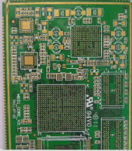
According to the product structure, FPC soft boards can be categorized as follows:
1. Single Side: This is the most fundamental type of FPC soft board. A conductive layer is applied over an adhesive layer, followed by a dielectric layer.
2. Double Side: This type features a double-sided substrate with an additional layer of covering film. However, due to increased thickness, flexibility is somewhat reduced, limiting its application field.
3. Multilayer: Comprised mainly of single-sided or double-sided boards, the conductive layers are interconnected through drilled holes. However, as the number of layers increases, flexibility diminishes, resulting in a more restricted application range.
4. Rigid-flex Board: This board combines multi-layer rigid boards with single-sided or double-sided FPC soft boards, offering the support of rigid boards alongside the flexibility of FPC soft boards.
5. Special Boards: This includes designs such as single-layer double-sided exposed boards (Double Access), embossed boards (Sculptural), and other unique variations.
Furthermore, for the integration of mobile and wearable devices, several advanced FPC types have emerged, including LCP-FPC with low dielectric constants, high-density multilayer FPCs, optical waveguide FPCs, waterproof FPCs, transparent FPCs, ultra-thin FPCs, and 3D forming FPCs. Additionally, integral molding FPCs and stretchable FPCs have become prominent. For instance, smartwatches or fitness bands utilize strap structures to integrate thin lithium polymer batteries, MEMS sensors, and FPCs, allowing for three-dimensional folding and embedding. Designs aimed at automotive electronics emphasize high shock and heat resistance in their FPCs.
To address trends in efficiency, high transmission rates, and sleek designs, high-speed connection interfaces like USB 3.0/3.1/HDMI are essential, offering transmission rates of 5–10Gbps. Telecom and Netcom equipment often require 20Gbps to fulfill optical fiber transmission needs, supporting high-speed applications. FPCs utilize low dielectric constant liquid crystal polymer (LCP) materials, complemented by ultra-thin copper foils with thicknesses of 6-9μm, achieving effective transmission while minimizing UHF transmission issues like skin effect, all while maintaining a thinner profile.
Laser drilling techniques, such as sky-eye drilling through copper foil/FR4, are employed to create HDI structures. As mobile devices and tablets advance towards higher clock speeds, multi-core architectures, and enhanced functionalities, the number of electronic components and contact pins per component has risen. This necessitates compliance with high-clock signal transmission requirements, attention to electrical characteristics, signal impedance, and the mitigation of skin effect. Moreover, to improve RF signal optimization and reduce electromagnetic interference, additional power and grounding layers must be incorporated, prompting a shift from traditional single-layer, double-layer, and four-layer designs to multi-layer PCBs and even high-density interconnect (HDI) PCBs.
HDI boards are produced using the build-up method. Typically, HDI boards employ primary build-up, while high-end variants utilize secondary (or further) build-up techniques, incorporating electroplating for hole filling and stacking, alongside advanced methods like laser direct drilling.
—
Let me know if you need any further adjustments!

