PCB Quality Assurance and Inspection Methods
Every electronic device today relies on PCBs for power and functionality. Designers have continuously improved PCB capabilities to support integrated circuits and meet compact size requirements.
Rigorous Quality Assurance
To ensure product quality and identify defects, PCB assembly (PCBA) suppliers conduct thorough quality assurance testing. Deficiencies in key characteristics can impact the entire manufacturing process and supply chain.

Common PCB Quality Inspection Methods
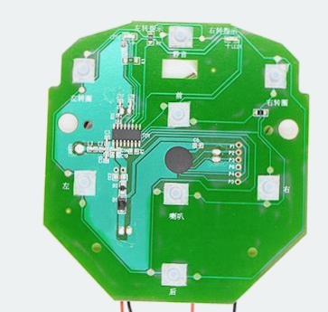
- Vision: Assemblers visually inspect boards for connections under well-lit conditions.
- Microscope: Handheld optical tools or USB microscopes are used for detailed examination.
- In-Circuit Testing: Capacitance testing methods include bed of nails and no-fixture testing.
- X-rays: Non-invasive method for inspecting PCB components.
- Sawing: Destructive but provides insights into assembly integrity.
- Automatic Optical Inspection (AOI): Cost-effective systems compare PCB images against reference boards.
- Functional Test: PCBs undergo self-checks to ensure functionality after manufacturing.
- Inspection Camera: High-resolution cameras allow for detailed inspection and analysis.
Quality Control Indicators
Final assembly inspection personnel are trained in key quality control indicators like Defects Per Unit (DPU) and Defects Per Million Opportunities (DPMO) to improve reliability and reduce complexity. Monitoring these metrics helps enhance product and process quality.
Optimizing PCB Layout for Better Circuit Performance
When designing a PCB, the lead engineer plays a crucial role in reviewing the layout and routing paths. One key aspect they consider is whether additional layers are necessary to enhance the circuit’s performance. By adding lamination strategically, the center of the board can be balanced along its z-axis, leading to improved functionality.
Furthermore, the final check involves meticulous attention to detail. This includes ensuring that nodes and circuits remain free from unnecessary noise, confirming the presence of a solder mask between pins and vias for added protection, and verifying that the screen printing is clear and legible for ease of use.
If you have any inquiries regarding PCB design or optimization, feel free to reach out to us at info@wellcircuits.com.