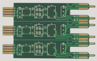
1. The definition of processing level is ambiguous.
In single-layer PCB design on the TOP layer, if the polarity is not clearly specified, it may lead to the board being mounted incorrectly on the device, resulting in poor soldering quality.
2. Excessive copper foil proximity to the outer frame.
The distance between extensive copper foil and the outer frame should be no less than 0.2mm. This is crucial because, during the milling process, if the milling reaches the copper foil, it can easily cause the foil to warp, leading to issues with solder mask adhesion.
3. Designing pads with filling blocks.
While designing pads with filling blocks may pass DRC checks during circuit design, it often fails in the manufacturing process. Consequently, solder mask layers cannot directly generate solder mask data. When solder mask materials are applied, the area occupied by the filling blocks will be covered, complicating the soldering of components.

4. The electric formation and flower pad connection
Due to the design of the flower pad power supply, the layers are oriented oppositely to the actual printed board, as illustrated above. All the lines serve as isolation lines. When creating multiple sets of power supply or different types of ground isolation lines, it is crucial to avoid leaving gaps that could short-circuit the two power supply sets or obstruct the connection area.
5. Misalignment of characters
Character pads on SMD soldering plates can complicate PCB testing and component soldering. If the character design is too small, it becomes challenging to screen print; if it’s too large, the characters may overlap, making them hard to read.
6. Short pads for surface mount devices
This issue arises during on-off testing, particularly for densely packed surface mount devices where the spacing between pins is minimal, and the pads are quite small. The test probes must be positioned in a staggered manner. If the pad design is too short, it won’t affect device installation but may hinder proper alignment of the test probes.
7. Aperture settings for single-sided pads
Single-sided pads typically do not require drilling. If holes are necessary, they should be marked, with the aperture designed to be zero. If a value is mistakenly assigned, the hole coordinates will be generated incorrectly in the borehole data. Single-sided pads should be clearly indicated if they require drilling.
8. Overlapping pads
During the drilling process, if the drill bit penetrates the same spot multiple times, it can break, damaging the hole. Overlapping holes in multilayer boards can lead to negative isolation drawings, resulting in scrap material.
9. Excessive filling blocks in design or very thin lines
The optical drawing data may be lost or incomplete. Since filling blocks are individually processed in optical data, an abundance of these blocks increases data processing difficulty and complexity.
10. Misuse of graphic layers
Some unnecessary lines have been added to various graphic layers, with over five lines designed for four layers, leading to confusion. This violates standard design practices. It is essential to keep graphic layers complete and clear during the design process.
In single-layer PCB design on the TOP layer, if the polarity is not clearly specified, it may lead to the board being mounted incorrectly on the device, resulting in poor soldering quality.
2. Excessive copper foil proximity to the outer frame.
The distance between extensive copper foil and the outer frame should be no less than 0.2mm. This is crucial because, during the milling process, if the milling reaches the copper foil, it can easily cause the foil to warp, leading to issues with solder mask adhesion.
3. Designing pads with filling blocks.
While designing pads with filling blocks may pass DRC checks during circuit design, it often fails in the manufacturing process. Consequently, solder mask layers cannot directly generate solder mask data. When solder mask materials are applied, the area occupied by the filling blocks will be covered, complicating the soldering of components.
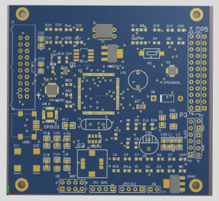
4. The electric formation and flower pad connection
Due to the design of the flower pad power supply, the layers are oriented oppositely to the actual printed board, as illustrated above. All the lines serve as isolation lines. When creating multiple sets of power supply or different types of ground isolation lines, it is crucial to avoid leaving gaps that could short-circuit the two power supply sets or obstruct the connection area.
5. Misalignment of characters
Character pads on SMD soldering plates can complicate PCB testing and component soldering. If the character design is too small, it becomes challenging to screen print; if it’s too large, the characters may overlap, making them hard to read.
6. Short pads for surface mount devices
This issue arises during on-off testing, particularly for densely packed surface mount devices where the spacing between pins is minimal, and the pads are quite small. The test probes must be positioned in a staggered manner. If the pad design is too short, it won’t affect device installation but may hinder proper alignment of the test probes.
7. Aperture settings for single-sided pads
Single-sided pads typically do not require drilling. If holes are necessary, they should be marked, with the aperture designed to be zero. If a value is mistakenly assigned, the hole coordinates will be generated incorrectly in the borehole data. Single-sided pads should be clearly indicated if they require drilling.
8. Overlapping pads
During the drilling process, if the drill bit penetrates the same spot multiple times, it can break, damaging the hole. Overlapping holes in multilayer boards can lead to negative isolation drawings, resulting in scrap material.
9. Excessive filling blocks in design or very thin lines
The optical drawing data may be lost or incomplete. Since filling blocks are individually processed in optical data, an abundance of these blocks increases data processing difficulty and complexity.
10. Misuse of graphic layers
Some unnecessary lines have been added to various graphic layers, with over five lines designed for four layers, leading to confusion. This violates standard design practices. It is essential to keep graphic layers complete and clear during the design process.

