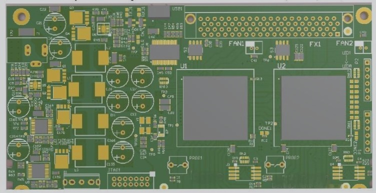
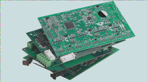
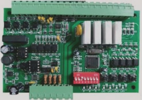
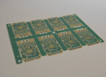
1. Random placement of text
1. The SMD solder pads for the text can complicate continuity testing of the printed board and hinder component soldering.
2. If the text is too small, it creates challenges for screen printing, while excessively large text may overlap, making it hard to read.
2. Misuse of the graphics layer
1. Some unnecessary connections appear on certain graphics layers. A four-layer board may end up designed with more than five layers of circuits, leading to confusion.

2. Simplify design processes. Using Protel software as an example, draw the traces on each layer with the Board layer and use it to mark these traces. This ensures that when light drawing data is generated, the unselected Board layer is omitted, preventing disconnections or short circuits from marked lines, thus maintaining the integrity and clarity of the graphics layer during design.
3. Avoid conventional design violations, such as placing component surfaces on the Bottom layer and solder surfaces on the Top, which can lead to complications.
Fourth, the overlap of pads
1. Pad overlap (excluding surface mount pads) indicates overlapping holes. During PCB drilling, this can lead to drill bit breakage from multiple drillings in a single spot, damaging the holes.
2. In multilayer boards, overlapping holes, such as an isolation disk and a connection pad, can cause issues, resulting in the film depicting the isolation disk and potentially creating scrap.
Fifth, setting single-sided pad apertures
1. Single-sided pads typically aren’t drilled. If drilling is necessary, the hole diameter should be set to zero. If a numerical value is used, drilling data will indicate hole coordinates, leading to complications.
2. Single-sided pads that require drilling should be explicitly marked.
Sixth, electrical ground as a flower pad and connection
Designing the power supply as a flower pad means the ground layer will visually oppose the actual printed board image, resulting in isolated lines for connections. Designers must be vigilant, especially when drawing isolation lines for multiple power supplies or grounds, to avoid gaps, short circuits, and blocked connection areas.
Seventh, drawing pads with filler blocks
Using filler blocks for pads can pass DRC inspections during circuit design, but poses challenges in processing. Such pads cannot directly generate solder mask data; during solder resist application, the filler block areas will be covered, making soldering difficult.
Eighth, unclear processing levels
1. If a single-sided board is designed on the TOP layer without clear front-back specifications, soldering components may become problematic.
2. In a four-layer board designed with TOP, mid1, mid2, and Bottom layers, incorrect layering during processing necessitates clarification.
Ninth, excessive filler blocks or thin filler lines
1. Excess filler blocks can lead to loss of Gerber data and incomplete files.
2. If filling blocks are drawn individually with lines, it can significantly increase the light drawing data volume, complicating data processing.
Tenth, surface mount device pads that are too short
For continuity testing in dense surface mount devices, the small spacing between pins necessitates staggered test pins (up and down or left and right). Short pad designs, while not impacting device installation, can interfere with proper test pin staggering.
Eleventh, inadequate spacing in large-area grids
The edges of lines forming large area grids should be spaced adequately (greater than 0.3mm). Insufficient spacing can lead to broken films adhering to the board during PCB manufacturing, causing wire breakage.


