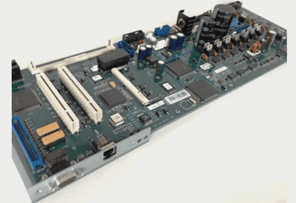
PCB Manufacturing Best Practices
- PCB Pad Processing:
- Material Selection:
- Sample Control:
- Review and Proofreading:
- Signal Arrangement:
- Communication and Detail Checking:
When it comes to PCB pad processing, methods such as immersion gold, anti-oxidation, and tin spraying are commonly used. While both lead-free and traditional tin spraying methods are effective, tin spraying offers a longer storage time. For screen printing colors, white and black are standard choices. When using a green solder mask, white text is preferred for clarity due to strong color contrast. Conversely, white solder text is best complemented with black lettering.
FR-4 is the go-to material for PCBs, especially for double-sided boards.
It is crucial to carefully control the number of samples in PCB proofing. Since proofing is usually done for small batch production, initial costs can be high, impacting overall expenses. To manage costs effectively, it is advisable for companies to calculate the NEE (Number of Expected Errors) before proofing and closely monitor sample and spare part assembly quantities.
Given the complexity of PCB proofing processes, selecting professional proofing manufacturers is key. It is essential to ensure that their processes align with design and manufacturing specifications. The configuration of processes should meet the company’s circuit board requirements and include robust anti-back-flying probe testing capabilities.
The logical arrangement of proofreading signals significantly impacts overall proofing quality. Paying attention to the completeness and reasonableness of signal layout, along with thorough checks of electrical components, enhances the PCB’s electrical performance, stability, and noise reduction.
Effective communication between PCB companies and proofing manufacturers is essential. When sending proofing materials, meticulous checking of document and component packaging is necessary to avoid missed deliveries. Neglecting minor details can result in subpar proofing outcomes.