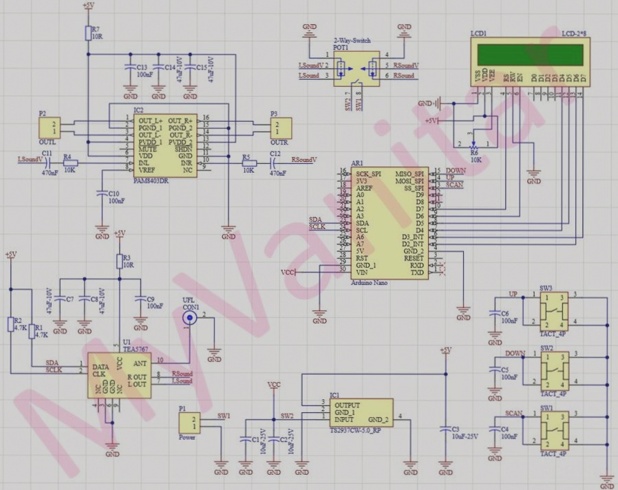
Essential Principles of PCB Design for Electronic Engineers
As semiconductor integration advances, custom PCBs remain crucial for specific applications, providing a physical platform for electronic designs. Here are ten critical design rules to enhance PCB layout and production:
Rule 1: Choose the Right Grid and Match it to Component Sizes
Select a grid system that aligns with common component sizes to optimize layout and prevent spacing issues. Consider the grid’s impact on copper fill for circuit board integrity.
Rule 2: Minimize Path Length and Directness
Prioritize short and direct routing, especially for analog and high-speed digital circuits, to reduce signal degradation and improve performance.
Rule 3: Utilize a Power Plane for Distribution
Maximize power plane usage for efficient power and ground distribution, reducing impedance and voltage drop for improved current delivery.
Rule 4: Group Components and Test Points
Cluster related components and test points for optimized performance and maintenance ease, enhancing electrical performance and troubleshooting efficiency.
Rule 5: Panelization for Cost Efficiency
Panelize PCB designs to reduce prototyping and manufacturing costs, aligning with manufacturer standards for space optimization and material cost reduction.
Rule 6: Standardize Component Values
Standardizing component values enhances design consistency, simplifies sourcing, and streamlines the assembly process.
Consolidating Component Values for Cost Efficiency
Standardizing component values within a narrow range can simplify your bill of materials (BOM) and lead to cost savings. As a designer, opting for components with similar performance but varying values allows for a more streamlined inventory. This not only reduces part costs but also improves long-term inventory management, benefiting designs with multiple PCB products.
Rule 7: Regular Design Rule Checks (DRC)
Conducting Design Rule Checks (DRC) frequently throughout the design process is crucial for maintaining a high-quality, error-free PCB layout. By running checks consistently, you can identify issues early on, saving time and effort in the long run. This proactive approach helps ensure design integrity and a smooth design phase.
Rule 8: Maximizing Screen Printing Benefits
Utilize screen printing on the PCB to provide valuable reference information for functions, test points, component orientations, and connector directions. Proper screen printing enhances communication between teams, simplifies production and testing processes, and is essential for assembly, debugging, and future servicing.
Rule 9: Importance of Decoupling Capacitors
Decoupling capacitors are crucial for filtering noise and maintaining stable power supply performance in your design. Including adequate decoupling capacitors, following standard values, and erring on the side of caution ensure optimal circuit stability. These inexpensive components are essential for reliable performance.
Rule 10: Verifying PCB Manufacturing Parameters
Prior to submitting design files for production, verify PCB manufacturing parameters to reduce the risk of costly mistakes and delays. Personally reviewing Gerber files using a free viewer helps catch errors and discrepancies early on. Ensuring that your design meets all manufacturing specifications guarantees a smoother production process and a higher-quality final product.