How to Detect and Prevent Common PCB Defects
1. One crucial factor to consider is whether the part itself includes a polarity symbol or if differences in appearance and shape can be utilized for identification.
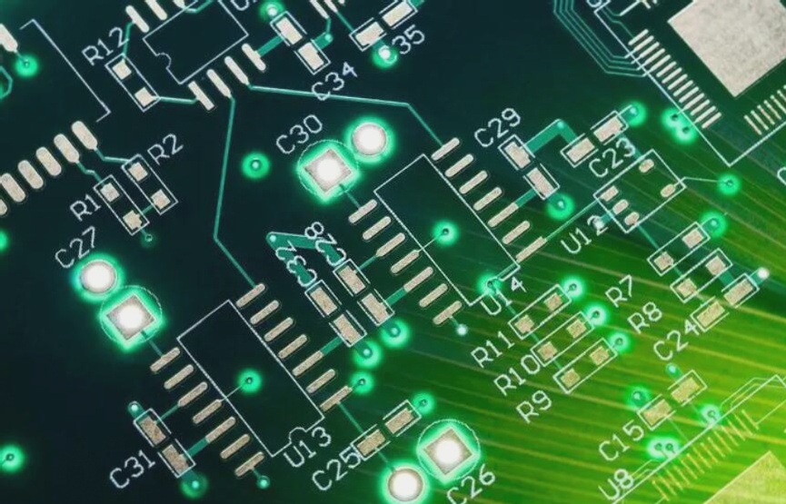
2. Detecting severe warping is relatively easier based on variations in light reflection intensity. However, identifying slight warping can be challenging. Advanced Optical Inspection (AOI) is effective in detecting severe deformations, while detecting minor warping depends on specific circumstances and parameter settings.
3. Although tin bridging is usually easy to spot, detecting it beneath a component presents challenges. In some cases, connectors may harbor hidden tin bridges under the component body, evading AOI detection.
4. To ensure quality, PCB production lines employ AOI, In-Circuit Test (ICT), and Functional Test (FVT). Some lines may also utilize Automatic X-ray Inspection (AXI) to inspect solder joints, especially for components like BGAs, using X-ray technology.