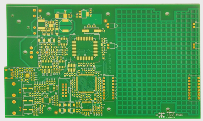
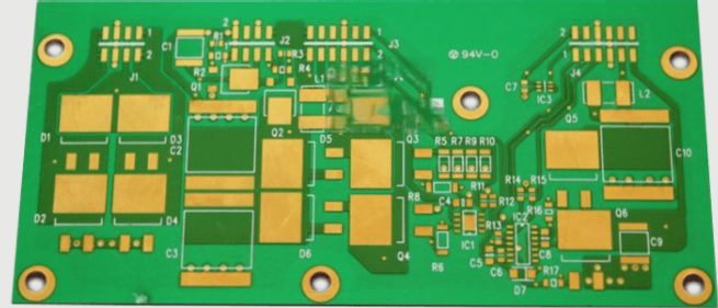
PCBA Foundry Substitutes: Lead-Free Processes and Advantages
- Leaded vs. Lead-Free Processes in PCBA Proofing
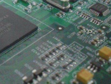
- Alloy Compositions: Leaded process uses 63/37 tin-lead composition, while lead-free process uses SAC 305 with Sn: 96.5%, Ag: 3%, and Cu: 0.5%. Lead-free process contains very low levels of lead, typically below 500 PPM.
- Melting Points: Lead-tin melting point ranges from 180° to 185°, while lead-free tin melts between 210° and 235°. With higher tin content, melting point and working temperature increase.
- Cost Variations: Tin is more expensive than lead, making lead-free processes significantly pricier. Costs for lead-free processes are about 2.7 times higher for wave soldering and manual soldering, with solder paste costs increasing by about 1.5 times.
- Process Differences: Lead and lead-free processes differ in solder, components, and equipment used, posing challenges for managing both simultaneously in small-scale PCBA processing plants.
- Advantages of PCBA Foundry Materials
- Lower Entry Barrier: Industry advancements have enabled a small PCB OEM model, reducing the MOQ requirement and allowing more companies to engage in OEM activities, thereby reducing production cycles.
- Reduced Management Costs: Foundry industry evolution offers options for small enterprises, adjusting costs based on customer orders rather than passing management costs directly to customers, enhancing acceptance and lowering operational barriers.
Explore more about PCBA processes and materials at wellcircuits.com.