Electroplating Processes for Multilayer PCBs
- Acid Bright Copper Electroplating
- Nickel/Gold Electroplating
- Tin Plating
Multilayer PCB Process Flow
The process flow for multilayer PCBs includes the following steps:
- Pickling
- Copper Plating on the Whole Board
- Pattern Transfer
- Acid Degreasing
- Secondary Countercurrent Rinsing
- Micro Etching
- Secondary Pickling
- Tin Plating
- Secondary Countercurrent Rinsing
- Countercurrent Rinsing
- Acid Dipping
- Graphic Copper Plating
- Secondary Countercurrent Rinsing
- Nickel Plating
- Secondary Water Washing
- Citric Acid Dipping
- Gold Plating
- Recovery
- 2-3 Stage Pure Water Washing
- Drying
Process Description
Pickling
Role and Purpose: Pickling removes oxide from the plate surface and activates it to prevent instability in sulfuric acid content.
Process Guidelines: Minimize acid leaching time to avoid surface oxidation and promptly replace the acid solution if needed.
Acid Specification: Use C.P grade sulfuric acid.
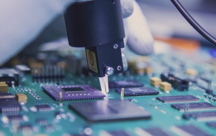
Full Plate Copper Plating
Function and Purpose: Protects the chemical copper layer and increases its thickness.
Process Parameters: The bath solution includes copper sulfate and sulfuric acid with specific content levels.
Process Maintenance: Daily and weekly maintenance tasks to ensure quality plating.
Major Treatment Procedure: Steps for major treatment to maintain plating quality.
Electroplating Process for PCB Manufacturing
Purpose of Acid Degreasing
- Remove oxide, residual ink, and glue from copper surface for better adhesion
- Use acid degreaser instead of alkaline for graphic circuit safety
- Maintain degreaser concentration at 10% with 6-minute processing time
Micro Etching for Copper Surface
- Clean and roughen copper surface to enhance bonding
- Use sodium persulfate for stable etching rate
- Maintain sodium persulfate concentration at 60 g/L for 20 seconds
Pickling Process
- Remove oxide and activate plate surface
- Use C.P grade sulfuric acid
- Avoid extended acid leaching times to prevent oxidation
Graphic Copper Plating
- Ensure required thickness for current load handling
- Thicken line and hole copper to specified dimensions
Electroplated Tin Application
- Protect circuit etching with electroplated pure tin
- Maintain stannous sulfate at 35 g/L and sulfuric acid at 10%
- Replenish tin plating additives daily based on kiloampere hours
- Follow maintenance procedures for optimal tin plating results
Major Treatment Procedure for Electroplated Tin
- Remove and clean anode periodically for maintenance
- Soak anode bag in alkaline solution and dilute sulfuric acid
- Perform tank liquid treatment with activated carbon powder
- Adjust chemical content based on analysis and replenish additives
Nickel Plating
The Importance of Nickel Plating in PCBs
Purpose and Benefits:
- Nickel plating serves as a vital barrier layer in PCBs, safeguarding against copper and gold layer diffusion. This protection is crucial for maintaining weldability and increasing the lifespan of the PCB.
- Moreover, nickel plating boosts the mechanical durability of the gold layer, ensuring the overall robustness of the PCB.
Enhancing PCB Performance with Nickel Plating Additives
Exploring the role of nickel plating additives in optimizing the functionality and reliability of printed circuit boards.