The Essential Components of a PCB Circuit Board
-
Circuit and Pattern (Pattern)
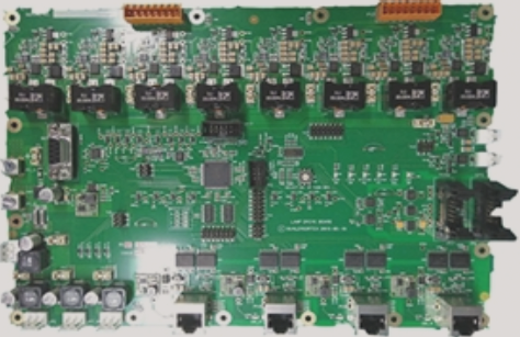
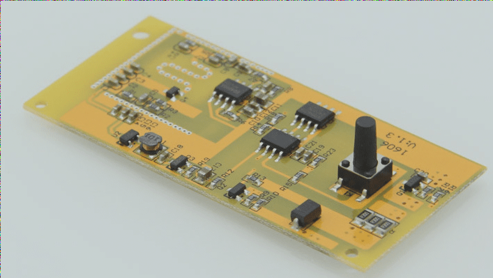
The circuit acts as a conductor between components, often including a large copper area for grounding and power. Routing and layout are created simultaneously during the design phase.
-
Dielectric Layer (Dielectric)
This layer is crucial for maintaining insulation between circuits and layers, also known as the substrate.
-
Holes (Through hole / via)
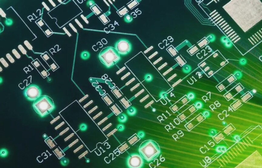
Through holes allow connections between traces on multiple levels. Larger through holes are used for component insertion, while non-through holes (nPTH) are employed for surface mount positioning and screw securing during assembly.
-
Solder Resistant / Solder Mask
Areas not requiring a tin coating are covered with insulating material (typically epoxy resin) to protect the copper from tin corrosion. This helps prevent short circuits between non-tinned circuits. Solder masks come in green, red, and blue variants.
-
Silk Screen (Legend / Marking / Silk Screen)
While not essential, silk screens label the names and positions of components on the board, aiding in maintenance and post-assembly identification.
-
Surface Finish
To prevent oxidation of copper surfaces, tinning areas must be protected for good solderability. Surface treatment methods include HASL, ENIG, Immersion Silver, Immersion Tin, and OSP.

Key Features of PCB Boards
-
High Density
PCB density has advanced with integrated circuit integration and mounting technology progress over the years.
-
High Reliability
Rigorous inspections and testing ensure PCBs can function reliably for up to 20 years.
-
Designability
Standardized design meets various performance requirements efficiently, reducing development times and enhancing efficiency.
-
Manufacturability
Modern practices enable standardized, scalable, and automated PCB production for consistent quality.
-
Testability
Comprehensive testing methods and standards evaluate PCB product eligibility and lifespan.
-
Assemblability
PCB products allow standardized component assembly and large-scale automation, enhancing production efficiency.
-
Maintainability
Interchangeable components in PCB products facilitate quick replacements during system failures, promoting rapid functionality restoration. Other benefits include miniaturization, weight reduction, and high-speed signal transmission.


