Due to the switching characteristics of switching power supplies, they often generate significant electromagnetic compatibility (EMC) interference. For power supply engineers, EMC engineers, and PCB layout engineers, understanding the causes of EMC issues is crucial. Layout engineers, in particular, must grasp methods to prevent the expansion of noisy areas. This article primarily focuses on key aspects of power supply PCB design.
1. Basic Relationships between Layout and PCB Design
– Several fundamental principles govern PCB layout:
– Every trace has impedance; current naturally follows paths with impedance.
– Radiation intensity correlates with current, frequency, and loop area.
– Common-mode interference relates to the mutual capacitance of high dv/dt signals to ground.
– Strategies for reducing EMI and enhancing immunity to interference are analogous.
2. Segment Layout According to Functionality
– Partition the layout into sections for power supply, analog, and high-speed digital components.
3. Minimize Di/dt and Dv/dt Loops
– Reduce the area and length (or width) of large di/dt loops.
– Enlarging trace width increases distributed capacitance (adjust width to minimize excess).
– Opt for straight traces to reduce enclosed areas and radiation.
4. Address Inductive and Capacitive Crosstalk
– Inductive crosstalk stems from large di/dt loops (loop antennas); mitigate by reducing mutual inductance (shrink loop areas and increase separation).
– Capacitive crosstalk arises from large dv/dt signals; reduce mutual capacitance by minimizing effective coupling areas and increasing separation (capacitance decreases with greater distance).
5. Utilize Loop Cancellation Principle
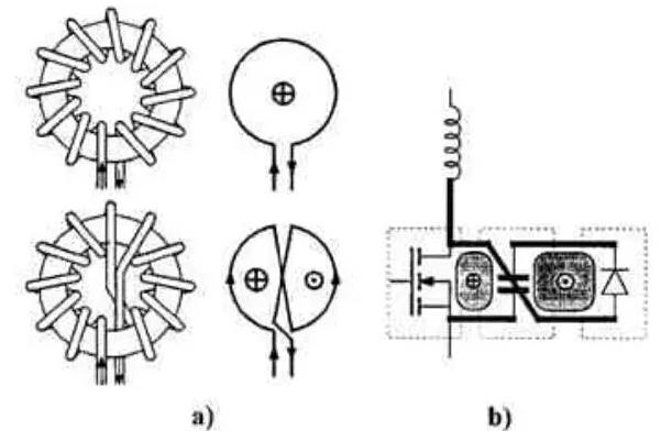
– Employ loop cancellation routing where possible to further diminish large di/dt loop areas.
– Similar to twisted pair configurations, this technique enhances anti-interference capabilities and extends transmission distances.
This revised version maintains the content while enhancing clarity and readability, focusing on practical tips for PCB layout engineers dealing with EMC challenges in switching power supplies.

6. Reducing the loop area not only mitigates radiation but also diminishes loop inductance, thereby enhancing circuit performance.
7. Reducing the loop area necessitates designing the return path for each trace.
8. When multiple PCB boards are interconnected via connectors, it’s crucial to ensure minimal loop area, especially for signals with high di/dt, high frequency, or sensitivity. Signal wires should ideally run close to corresponding ground wires, with twisted pairs used where necessary (ensuring each pair’s length corresponds to a multiple of the noise half-wavelength). For instance, inside a computer case, the USB interface between the motherboard and front panel utilizes twisted pair cables, underscoring their role in minimizing interference and radiation.
9. For data cables, incorporating additional ground wires evenly distributed throughout can effectively reduce loop area.
10. Despite some inter-board connections carrying low-frequency signals, improper handling can lead to significant emission of high-frequency noise through both conduction and radiation.
11. When routing traces, prioritize high-current paths and those prone to radiation.
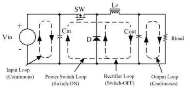
12. Switching power supplies typically feature four distinct current loops—input, output, switch, and freewheeling. While input and output loops are nearly direct current with minimal EMI, they are susceptible to disturbances. In contrast, switch and freewheeling loops exhibit higher di/dt and require careful attention.
13. The gate drive circuit for MOS (IGBT) transistors also tends to generate substantial di/dt.
14. To prevent interference, avoid placing small signal circuits (e.g., control and analog circuits) within proximity of high-current, high-frequency, or high-voltage circuits.
15. Minimize loop area and trace length for sensitive signal circuits to reduce interference.
16. Position small signal traces away from lines with large dv/dt (such as switch tube C and D poles), and ensure good grounding contact with the ground plane. Additionally, maintain distance from lines with large di/dt to prevent inductive crosstalk. Avoid routing small signal traces beneath traces with large dv/dt. Grounding the back of small signal traces (to the same ground) can further reduce coupled noise.
17. An effective strategy involves surrounding and backing large dv/dt and di/dt signal traces (including switch device C/D poles and heat sinks) with ground layers on upper and lower PCB layers. Use vias to connect these grounds to a common low-impedance point (typically switch tube E/S pole or sampling resistor) to minimize radiated EMI. Ensure that the ground for small signals remains separate to avoid increased interference. Surface-mounting switching devices can reduce mutual capacitance and coupling.
18. Avoid using vias for traces prone to interference, as vias interfere with all layers they traverse.
19. Shielding can reduce radiated EMI but may increase conducted EMI due to added capacitance to ground. Proper grounding of shielding layers mitigates this effect and should be carefully considered during design.
20. To mitigate common impedance interference, implement single-point grounding and power supply.

21. Switching power supplies typically feature three grounds: the input power high current ground, output power high current ground, and small signal control ground. The diagram below illustrates their connection method.
22. When grounding, the nature of the ground should be assessed first before making connections. Sampling and error amplification grounds should usually connect to the negative pole of the output capacitor. Sampling signals are generally taken from the positive pole of the output capacitor to minimize common impedance interference. The control and drive grounds of the IC are typically not led out separately. Hence, the lead impedance of the sampling resistor to the above ground must be minimized to reduce common impedance interference and enhance current sampling accuracy.
23. The output voltage sampling network should be placed near the error amplifier rather than the output. This approach leverages low-impedance signals, which are less susceptible to interference compared to high-impedance signals. Ensure that sampling traces are closely routed to mitigate noise pickup.
24. Pay attention to the layout of inductances, ensuring they are positioned far apart and perpendicular to each other to minimize mutual inductance. This is particularly critical for energy storage and filter inductances.
25. When using high-frequency and low-frequency capacitors in parallel, prioritize placing high-frequency capacitors closer to the user.
26. Low-frequency interference typically manifests as differential mode (below 1M), while high-frequency interference is generally common mode and often radiatively coupled.
27. If high-frequency signals couple to input leads, they may lead to EMI (common mode). Placing a magnetic ring close to the power supply on the input lead can mitigate this issue. Persistent EMI indicates the need to address either coupling reduction or circuit EMI reduction through improved filtering, buffering, or clamping.
28. Measurement of differential mode and common mode currents is crucial.
29. Position the EMI filter as close as possible to the incoming line and keep incoming line routing as short as feasible to minimize coupling between stages. Shield the incoming line with chassis ground as previously described. Similarly treat the output EMI filter. Maintain a distance between incoming lines and high dv/dt signal traces during PCB layout considerations.


