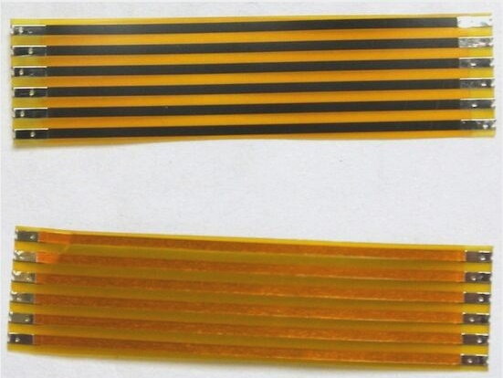
The flexible PCB substrate consists of an insulating base material, an adhesive, and a copper conductor. Once the circuit is created through lithography, a protective covering film must be applied to prevent oxidation of the copper circuit and safeguard it from environmental temperature and humidity. This cover film is made up of an insulating substrate and an adhesive. Polyester (PET) and Polyimide (PI) are the most common insulating base materials for flexible circuit boards, each offering distinct advantages and disadvantages. PET is more cost-effective, while PI provides superior reliability. Currently, various companies are developing alternative materials, such as PBO from Dow Chemical, and PIBO and LCP from Kuraray. Adhesives are typically employed for flexible circuit board substrates, but the thermal properties and reliability of existing adhesive materials are lacking. Therefore, removing the adhesive could enhance electrical and thermal properties. Additionally, in terms of cover film material technology, traditional methods use non-optically sensitive materials. Before applying this protective film, mechanical drilling is required to create contacts, solder pads, and guide holes, generally achieving only 0.6 to 0.8 mm in diameter. This precision is inadequate for flexible boards that support components, as future guide hole diameters will need to reach 50 μm. Using a photosensitive cover film could improve resolution to below 100 μm.
At present, the demand for long-term product reliability and the application of thinner, load-bearing components is driving the increase of non-adhesive flexible substrates. These substrates represent the future trend in flexible materials, with three primary manufacturing methods: (1) Sputtering/Plating; (2) Coating (Cast); (3) Hot pressing (Lamination). Each method has its unique advantages and disadvantages, with the manufacturing processes detailed as follows:
1. **Sputtering/Electroplating Method**: This approach uses a PI film as the substrate, where a thin layer of copper (less than 1μ) is initially sputtered. The circuit is then etched using photolithography, followed by electroplating on the copper circuit to achieve the desired thickness, akin to the semi-additive method used in circuit boards.
2. **Coating Method**: Utilizing copper foil as the base material, a thin layer of high-order PI resin is first coated. After high-temperature curing, a thicker layer of PI resin is applied to enhance the substrate’s rigidity, forming a two-layer (2L) structure. This method requires two coating steps, resulting in higher process costs. To mitigate these costs, two strategies can be employed: precision coating technology allows simultaneous double-layer coating, reducing manufacturing steps, while developing a single-layer PI resin formula can replace the double-layer approach, providing adhesion and stability while simplifying the process.
3. **Hot Pressing Method**: In this method, a thin layer of thermoplastic PI resin is first coated onto PI film, which is then hardened at high temperature. A copper foil is placed on the hardened thermoplastic resin, followed by the application of high temperature and pressure to remelt the thermoplastic PI and bond it with the copper foil to form a 2L structure.
Currently, no single process meets all needs, so the choice depends on the PCB designer’s material selection and thickness requirements. The coating method offers a good balance between cost and properties, providing excellent adhesion, high conductor selectivity, and the possibility of a very thin substrate. Few manufacturers can produce double-sided processes due to their complexity; however, in 1999, the output of double-sided coatings exceeded 970,000 square meters. According to TechSearch International, the estimated global monthly output in 2000 was around 220,000 square meters, with the sputtering method being the most commonly used.
Currently, PICs are available in two forms: dry film and liquid film. Dry film’s advantages include being solvent-free and easier to manufacture, although it is more expensive per unit area and less resistant to chemicals. Liquid PICs require coating machines but are more cost-effective, making them suitable for mass PCB production. Substrates include Acrylic/Epoxy and PI. TechSearch statistics indicate that Epoxy-based liquid PIC currently holds the largest market share, exceeding 70%, with Nippon Polytech/Rogers leading at 44%, followed by Nitto Denko at 21%, and DuPont at 18%. Liquid PI is known for its excellent heat resistance and insulation properties, making it ideal for high-end IC packages.