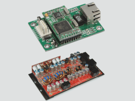
Essential Considerations for PCB Design
When designing PCBs for electronic systems, it is crucial to address anti-interference requirements upfront to save time and avoid unnecessary detours. By focusing on three primary elements that contribute to interference, you can enhance the effectiveness of your PCB design:
1. Interference Source
The interference source, represented as du/dt mathematically, includes components like lightning, relays, motors, and high-frequency clocks. High di/dt values indicate strong interference sources.
2. Propagation Path
The propagation path defines how interference travels from the source to sensitive devices. It can occur through conduction via wires or radiation through space.
3. Sensitive Devices
Components like A/D and D/A converters, microcontrollers, and digital ICs are vulnerable to interference and require protection.
Key Principles of Anti-Interference PCB Layout Design
- Suppressing interference sources
- Interrupting interference propagation paths
- Enhancing the resistance of sensitive devices to interference
1. Suppressing Interference Sources
Reducing du/dt and di/dt of the interference source is crucial. Common methods include using capacitors, inductors, and resistors to mitigate interference.
Common Measures to Suppress Interference Sources:
- Relay Coils: Utilize freewheeling diodes to eliminate back electromotive force interference.
- Spark Suppression: Implement an RC series circuit to reduce electric spark impact.
- Motor Filtering: Add a filter circuit to the motor for optimal performance.
- ICs on the PCB: Pair each IC with high-frequency capacitors for power supply filtering.
- Avoid 90-Degree Bends: Reduce high-frequency noise emissions by avoiding sharp bends in signal traces.
- Thyristors: Connect RC suppression circuits to reduce noise and prevent breakdown.
Interference Categorization
Interference can be conducted through wires or radiated through space. Conducted interference can be mitigated with filters, while radiated interference requires increased distance and shielding.
Enhancing Anti-Interference Performance for Sensitive Devices
- Consider Power Supply Impact: Effective power management can significantly enhance the circuit’s anti-interference capability. Incorporate filter circuits or voltage regulators to minimize power supply noise, such as using a π-shaped filter circuit with magnetic beads and capacitors.
- Optimize Crystal Oscillator Layout: Place the crystal oscillator close to the microcontroller, isolate the clock area with a ground wire, and ensure proper grounding for improved performance.
- Segment Circuit Board Properly: Segregate strong and weak signals, digital and analog signals, and keep interference sources away from sensitive components like microcontrollers.
- Separate Digital and Analog Areas: Use separate ground wires for digital and analog sections, connecting them to the power ground at a single point. This practice should extend to A/D and D/A chips.
- Ground High-Power Devices Independently: Ground the microcontroller and high-power devices separately to minimize mutual interference. Place high-power devices at the board edges when possible.
- Utilize Anti-Interference Components: Incorporate magnetic beads, ferrite rings, power filters, and shields in critical areas to enhance the circuit’s resistance to interference.
Strategies for Anti-Interference Performance Improvement
Improving the anti-interference performance of sensitive devices involves reducing interference noise pickup and ensuring quick recovery from abnormal conditions. Key strategies include:
- Minimize trace loop area to reduce induced noise.
- Use thicker power and ground wires for reduced voltage drops and coupling noise.
- Avoid leaving unused I/O ports floating; connect them to ground or the power supply. Ground or connect idle terminals on ICs without altering system logic.
- Integrate power supply monitoring and watchdog circuits like IMP809, IMP706, IMP813, X25043, and X25045 for enhanced anti-interference capabilities.
- Reduce microcontroller clock frequency and opt for lower-speed digital circuits to lower susceptibility to noise if feasible.
- In PCB designs, solder IC devices directly onto the board, minimizing the use of IC sockets.
If you have any PCB-related questions, feel free to reach out to us at info@wellcircuits.com.