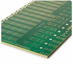
Avoiding Right-Angle Traces in PCB Layout
When it comes to PCB layout, avoiding right-angle wiring is crucial as it directly impacts signal transmission quality. The presence of right-angle traces can lead to impedance discontinuities, affecting signal integrity. It’s not just right-angle traces but sharp-angle traces as well that can cause impedance variations.
Key Factors Affecting Signal Transmission
- The corner of a right-angle trace acts as a capacitive load, slowing down the rise time of signals.
- Impedance mismatches at right-angle traces result in signal reflections.
- Right-angle tips can generate electromagnetic interference (EMI), further disrupting signal transmission.
Calculating the parasitic capacitance introduced by the right angle can be done using the formula: C=61W(Er)^1/2/Z0, where C is the equivalent capacitance in picofarads, W is the trace width in inches, εr is the dielectric constant, and Z0 is the characteristic impedance. As the line width of the right-angle trace increases, impedance decreases, leading to signal reflection.
Reflection Coefficient Calculation
By determining the equivalent impedance with the increased line width and using the reflection coefficient formula ρ=(Zs-Z0)/(Zs+Z0), we can quantify the impact of right-angle wiring. Typically, the impedance change ranges from 7% to 20%, with a maximum reflection coefficient of around 0.1.


