Via Design Considerations in High-Speed PCBs
Vias play a crucial role in multilayer PCBs, with drilling costs typically making up a significant portion of manufacturing expenses. Each hole in a PCB serves as a via, connecting different layers of the board.
1. Understanding Vias’ Parasitic Capacitance
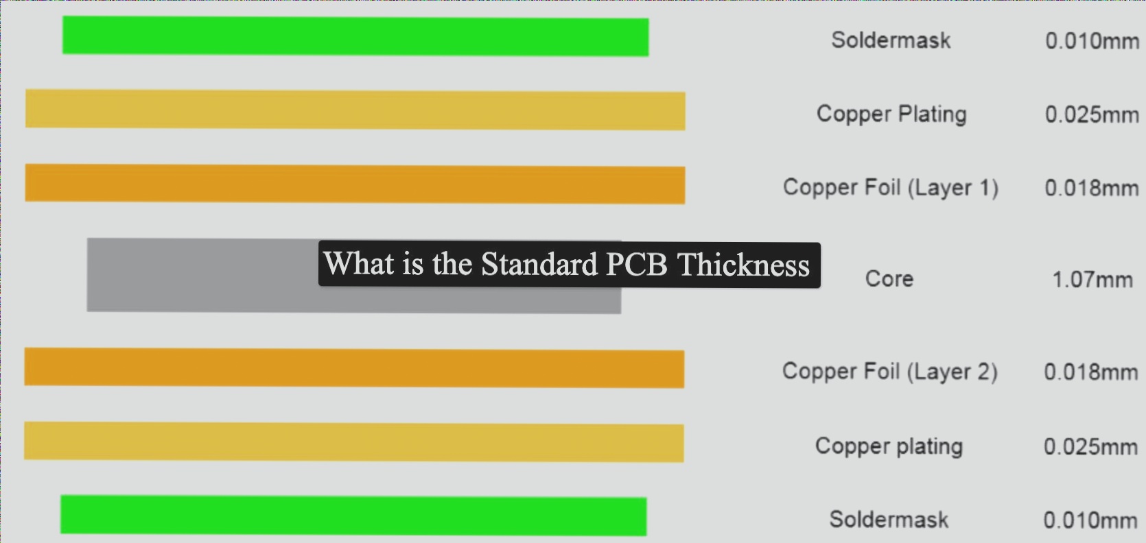
Vias exhibit parasitic capacitance to the ground, impacting signal integrity and circuit performance. By considering factors like isolation hole diameter, via pad diameter, board thickness, and dielectric constant, designers can estimate the parasitic capacitance of a via. This capacitance can affect signal rise time and circuit speed, necessitating careful consideration, especially when multiple vias are used in high-speed traces.
2. Addressing Vias’ Parasitic Inductance
In addition to capacitance, vias also demonstrate parasitic inductance, which can have a more significant impact in high-speed digital circuits. The parasitic inductance of vias can affect bypass capacitor efficiency and overall power system filtering. Designers can calculate the approximate inductance of a via to understand its impact on signal integrity and impedance, particularly in scenarios involving high-frequency currents.
3. Practical Design Strategies for Vias in High-Speed PCBs
- Choose via sizes carefully to balance cost and signal quality, considering factors like layer count and board density.
- Opt for thinner PCBs to reduce parasitic capacitance and inductance in vias.
- Position power and ground pins close together with short leads to minimize inductance and impedance.
- Avoid unnecessary layer changes and vias in signal traces to maintain signal integrity.
- Strategically place grounded vias near signal vias to optimize signal loops and consider adding redundant ground vias for enhanced performance.
WellCircuits Limited: Your Partner in High-Precision PCB Solutions
WellCircuits Limited specializes in manufacturing high-precision double-sided and multi-layer PCBs, including impedance-controlled boards, blind buried vias, and thick copper circuits. Their product range features HDI, thick copper, backplanes, rigid-flex combinations, buried capacitance, Golden Finger, and other specialized circuit board types tailored to diverse customer needs.


