During the design and manufacturing process of PCBs, various factors such as material properties, manufacturing processes, and environmental conditions can influence the electrical characteristics of the PCB, thereby affecting its performance. Therefore, it is essential to implement corresponding compensation measures to ensure PCB stability and reliability.
Below are common production compensations employed by Wellcircuits in PCB manufacturing:
Trace Compensation
1. Reason for Trace Width Compensation
After electroplating, trace etching involves both horizontal and vertical (side) etching due to trace thickness. Thus, compensation is necessary to offset side etching, ensuring trace integrity. The side etching process is illustrated below:

2. Industry Standards for Trace Width Compensation
Compensation for 1oz copper thickness:

Compensation adjustments can impact spacing; for example, if the original line-to-copper foil spacing is 4 mil, a 0.3 mil compensation on each side results in a final spacing of 3.4 mil. Adjustments ensure compliance with production capabilities.
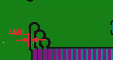
To maintain trace integrity, engineers may remove excess copper foil, modifying customer-provided files accordingly.
Drill Compensation
1. Reason for Drill Compensation
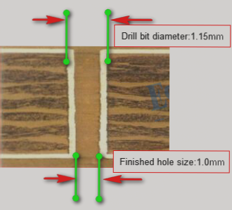
Gerber files specify finished hole sizes, which reduce during PCB production due to interior plating. Drill compensation ensures final hole size meets requirements.
For example, a 1.00mm finished hole size requires a 1.15mm drill bit considering immersion gold and IPC standard Class II.
2. Industry Standards for Drill Compensation
Compensation values adhere to established production capacity test results, generally uniform across the industry.
Pad Compensation
Designing pads accounts for manufacturing errors to ensure reliable connections and soldering quality. Methods include:
a. Diameter compensation: Adjusting pad diameter within 10% based on component requirements.
b. Shape compensation: Altering pad shape (e.g., circular to square) to fit components.
c. Spacing compensation: Adjusting pad spacing relative to component pin width.
Consideration of soldering processes and design ensures quality connections.
Material Compensation
Compensating for material expansion and contraction during PCB production maintains dimensional stability:
a. Thermal expansion coefficients influence PCB size; compensation aligns with selected materials.
b. PCB diagram size and material selection affect final PCB dimensions.
c. Manufacturing process parameters (e.g., temperature, humidity) stabilize PCB dimensions.
Material compensation safeguards PCB integrity throughout production.
Electrical Characteristic Compensation
Compensating for impedance, capacitance, and other electrical characteristics optimizes PCB performance:
a. Resistance compensation adjusts for substrate materials and trace characteristics.
b. Capacitance compensation adapts to trace geometry and wiring methods.
c. Signal delay and impedance matching compensation ensure timing and signal integrity.
These measures enhance PCB circuit stability and reliability.
Interactions among compensation measures necessitate comprehensive design adjustments, considering practical applications and manufacturing constraints.
If you have any questions about PCB or PCBA, please contact us at info@wellcircuits.com.

