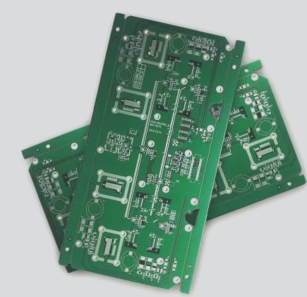
The Challenge of Test Points on Shrinking PCBs
As technology advances, printed circuit boards (PCBs) are shrinking in size, posing a challenge for accommodating electronic components. The issue of test points occupying valuable PCB space is a common concern for design and manufacturing teams.
Limitations of Needle Bed Testing
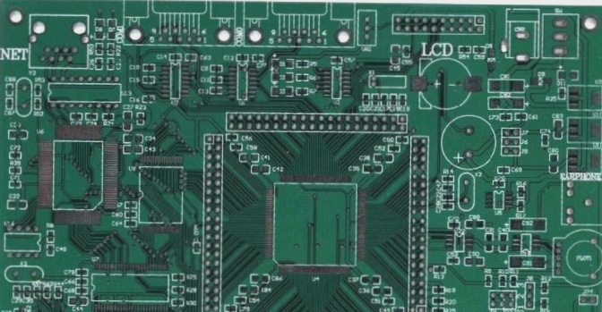
Needle bed testing, while common, has its limitations. Probes must meet a minimum diameter to avoid breakage, and spacing between needles is crucial to prevent short circuits and cable interference. Taller components can also pose challenges, requiring modifications to the needle bed layout.
Exploring Alternative Testing Methods
With the push to reduce test points, alternative testing methods like Net test, Test Jet, Boundary Scan, and JTAG have emerged. While AOI and X-Ray methods aim to replace traditional needle bed testing, none can fully replace In-Circuit Test (ICT).
Consulting Fixture Manufacturers for ICT Implementation
Before implementing ICT needle testing, it’s essential to consult with fixture manufacturers. They can provide guidance on probe diameter and test point spacing requirements to ensure the integrity of the testing process and prevent fixture damage.