
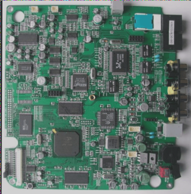
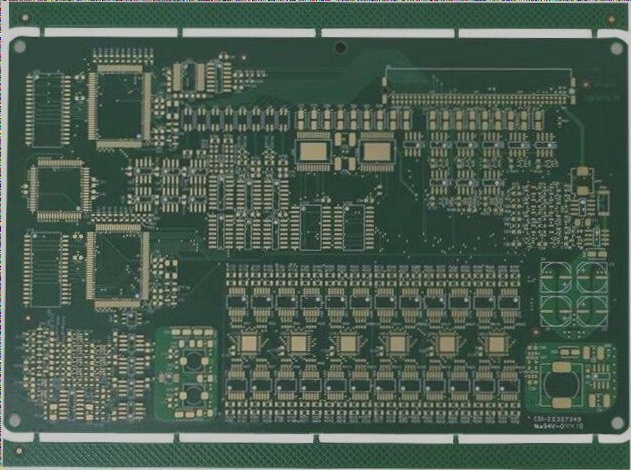
PCB Design Checklist for Electronic Engineers
- 1) Analyze the circuit to ensure smooth signal flow
- 2) Use short or isolated signal paths when necessary
- 3) Shield critical areas effectively
- 4) Utilize basic grid graphics
- 5) Optimize the PCB size
- 6) Maximize trace widths and spacing
- 7) Use preferred pad and hole sizes
- 8) Prepare PCB artwork and silkscreen appropriately
- 9) Minimize jumpers and avoid passing through components

Additional Inspection Items:
- 10) Ensure visibility and correctness of letters after assembly
- 11) Prevent copper foil blistering with appropriate windows
- 12) Include tool positioning holes
Electrical Characteristics Inspection:
- 1) Analyze wire resistance, inductance, and capacitance influences
- 2) Check wire accessory spacing for insulation requirements
- 3) Control insulation resistance in key areas
- 4) Fully identify polarity
- 5) Measure wire spacing impact on leakage resistance and voltage
- 6) Identify surface coating medium changes
Physical Characteristics Inspection:
- 1) Ensure pads and positions are suitable for assembly
- 2) Verify PCB can withstand shock and vibration
- 3) Determine spacing for standard components
- 4) Securely fix loose or heavy components
- 5) Correct heat dissipation and isolation
- 6) Position multi-lead components accurately
- 7) Eliminate potential interferences
- 8) Verify component arrangement and orientation
- 9) Check positioning hole sizes
- 10) Ensure comprehensive tolerances
- 11) Control physical properties of coatings
- 12) Maintain acceptable hole-to-lead wire ratios
Mechanical Design Factors:
PCBs provide mechanical support but should not be structural parts. Support every 5 inches on the PCB edge is recommended.
Installation Requirements:
Support should extend at least 1 inch from all edges. For different thicknesses, adjust support point distances for rigidity and resonance prevention.
Mounting Technologies Considerations:
- 1) PCB size and shape
- 2) Input and output terminals
- 3) Available equipment space
- 4) Loading and unloading ease
- 5) Attachment types
- 6) Heat dissipation needs
- 7) Shieldability requirements
- 8) Circuit interactions
Mounting Frames Requirements:
- 1) Ensure no component obstruction
- 2) Consider installation distances between PCBs
- 3) Design with appropriate mounting holes and slots
- 4) Account for plug-in tool sizes
PCB Assembly Tips for Plug-in Devices
- Attach plug-in devices securely to the PCB assembly using rivets.
- Design mounting frames with load-bearing flanges for PCBs.
- Ensure compatibility between plug-in tools and PCB size, shape, and thickness.
- Consider costs associated with plug-in tool usage, including tool price and additional expenses.
- Ensure sufficient equipment access for plug-in tool fastening and use.
When working on PCB assembly, it is crucial to follow these guidelines to ensure proper functioning and longevity of your electronic devices. By securely attaching plug-in devices and designing suitable mounting frames, you can enhance the performance and durability of your PCBs. Additionally, considering compatibility and costs associated with plug-in tools will help you make informed decisions during the assembly process. Remember to prioritize equipment access for efficient fastening and use of plug-in tools.
 العربية
 简体中文
简体中文 Nederlands
 English
 Français
 Deutsch
 Italiano
 日本語
日本語 한국어
한국어 Português
 Русский
 Español
 ไทย
ไทย