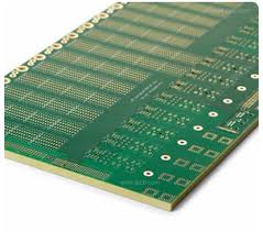
The research and development speed of LED switching power supply has made a significant technological leap in recent years, and the speed of new product upgrading has also accelerated a lot. As the last design link, the PCB design is also particularly important, because once there is a problem in this link, it is likely to generate more electromagnetic interference to the entire LED switching power supply system, which will have adverse effects on the stability and safety of the power supply. So, what is the correct way to design a PCB?
The results of component layout research and market practice of LED power supply in recent years have proved that even if the circuit schematic diagram designed in the early stage of research and development is very correct, once there is a problem with the PCB design, it will be detrimental to the reliability of electronic equipment. Influence, such as the interference caused by the lack of consideration of power supply and ground wire, will reduce the performance of the product, so when designing the PCB board, it is necessary to adopt the correct method.
In a PCB board commonly used in switching power supplies, usually each switching power supply has four current loops, which are the input signal source current loop, the power switch AC loop, the output rectifier AC loop, and the output load current loop. The input loop charges the input capacitor through an approximate DC current, and the filter capacitor mainly plays the role of broadband energy storage. Similarly, the output filter capacitor is also used to store high-frequency energy from the output rectifier while removing DC energy from the output load loop. Therefore, the terminals of the input and output filter capacitors are very important, and the input and output current loops should only be connected to the power supply from the terminals of the filter capacitors, respectively.
The setting and connection of input and output loops are very important for the entire printed circuit board, and their rationality will be directly related to the magnitude of electromagnetic interference. If the connection between the input and output circuits and the power switch and rectifier circuit cannot be directly connected to the terminals of the capacitor, the AC energy will be radiated into the environment by the input or output filter capacitor. The AC loop of the power switch and the AC loop of the rectifier contain high-amplitude trapezoidal currents. The harmonic components in these currents are very high. The frequency is much higher than the fundamental frequency of the switch. about 50ns. These two loops are the most prone to electromagnetic interference, so these AC loops must be routed before other traces in the power supply.
In the input and input loops of the LED switching power supply, each loop is composed of three main components, which are filter capacitors, power switches or rectifiers, inductors or transformers. These three important components should be placed next to each other, and the components should be positioned so that the current path between them is as short as possible. The best way to build a switching power supply layout is similar to its electrical design, the best design flow is as follows: place the transformer → design the power switching current loop → design the output rectifier current loop → control circuit connected to the AC power circuit → design the input current source loop and input filter.