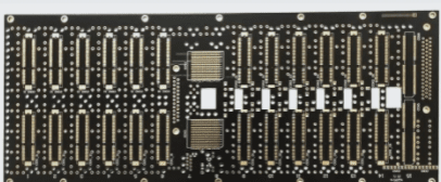
Common Mistakes in PCB Schematics:
- Missing signal connection to the pin in the ERC report:

Ensuring proper connections in PCB schematics is crucial for the functionality of electronic devices. Here are some common errors to avoid:
- Inconsistent grid attributes can lead to unconnected pins and wires when components are placed.
- Reversing the pin direction or not connecting the non-pin name end when creating a component.
- Components extending beyond the drawing boundary due to improper placement.
- Partial import of the network table into the PCB due to global settings not being selected.
- Avoiding the use of the annotate feature when working with self-created multi-part components.
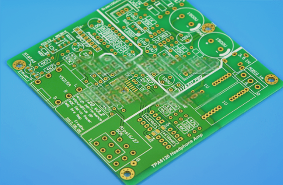
Common PCB Errors:
- NODE not found when loading the netlist:
Issues with component packages and library consistency can lead to errors in PCB design:
- Components using packages not present in the PCB library.
- Inconsistent package names between schematic and PCB library.
- Mismatched pin numbers between schematic and PCB library for components.
- Unable to print everything on one page:
Printing issues can arise due to improper PCB setup:
- PCB library not created at the origin.
- Objects outside the PCB boundary due to multiple movements and rotations.
- The DRC report indicates that the network is split into multiple parts:
Properly connecting the network is essential for PCB functionality:
- Use the CONNECTEDCOPPER command to address network split issues.
When working on PCB designs, it’s important to pay attention to routing to ensure proper functionality. Effective routing is key to a successful PCB design, and different methods can be utilized based on project requirements.
Routing methods include automatic routing and interactive routing, each with its own set of considerations. Ground wires and layer positioning play a significant role in minimizing interference and ensuring signal integrity.