1. **Reasonably Divide Functional Areas**
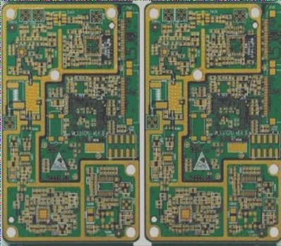
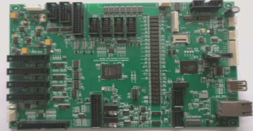
When conducting reverse engineering on the schematic diagram of a well-designed PCB, a thoughtful division of functional areas can assist engineers in minimizing unnecessary challenges and enhancing drawing efficiency. Typically, components with similar functions on a PCB are grouped together, and this functional area segmentation provides a reliable and precise framework for schematic inversion.
However, this functional area division is not arbitrary. Engineers need a solid understanding of electronic circuit principles. Start by identifying the core component within a specific functional unit, then trace the wiring connections to locate other components belonging to the same functional unit, thereby establishing a functional partition. The creation of these functional partitions serves as the foundation for schematic drawing. Additionally, during this process, don’t overlook the clever use of the component serial numbers on the circuit board, as they can facilitate quicker functional partitioning.

2. Find the appropriate reference parts
The reference part can be described as the primary component used in the initial schematic design of the PCB net. Once the reference part is established, the schematic can be drawn according to the pins of these parts, which greatly enhances the accuracy of the schematic representation.
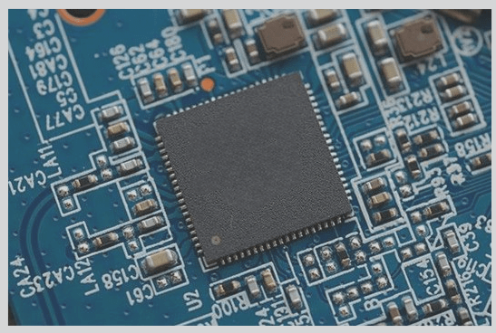
For engineers, selecting reference parts is generally straightforward. Typically, components that play a significant role in the circuit are chosen as reference parts. These components are usually larger and have more pins, making them easier to draw. Suitable examples include integrated circuits, transformers, and transistors.
3. Distinguish lines correctly and wire logically
Engineers must possess relevant knowledge about power supplies, circuit connections, and PCB wiring to differentiate between ground wires, power wires, and signal wires. This distinction can be analyzed based on component connections, the width of the circuit’s copper traces, and the specific characteristics of the electronic product.
In the wiring diagram, to prevent line crossings and overlaps, multiple grounding symbols can be utilized for ground lines. Different colors and styles can be employed for various lines to ensure clarity and easy identification. Additionally, special symbols can be used for various components, or unit circuits can be drawn separately and then combined.
4. Understand the basic framework and study similar schematics
Engineers should be proficient in the composition of basic electronic circuit frameworks and drawing principles, enabling them to create simple and classic unit circuits while forming the overall structure of electronic circuits.
Furthermore, it’s important to recognize that similar electronic products often share schematic characteristics. Engineers can leverage their experience and learn from analogous circuit diagrams to effectively reverse-engineer the schematics of new products.
5. Verify and optimize
Once the schematic is completed, the reverse design of the PCB schematic can be regarded as finalized after thorough testing and verification. The nominal values of components sensitive to PCB distribution parameters must be checked and optimized. A comparison and analysis of the schematic against the PCB file diagram are necessary to ensure full consistency between the two.
The above outlines the reverse engineering steps for the PCB schematic and highlights key details to consider.
If you have any PCB manufacturing needs, please do not hesitate to contact me.Contact me
When conducting reverse engineering on the schematic diagram of a well-designed PCB, a thoughtful division of functional areas can assist engineers in minimizing unnecessary challenges and enhancing drawing efficiency. Typically, components with similar functions on a PCB are grouped together, and this functional area segmentation provides a reliable and precise framework for schematic inversion.
However, this functional area division is not arbitrary. Engineers need a solid understanding of electronic circuit principles. Start by identifying the core component within a specific functional unit, then trace the wiring connections to locate other components belonging to the same functional unit, thereby establishing a functional partition. The creation of these functional partitions serves as the foundation for schematic drawing. Additionally, during this process, don’t overlook the clever use of the component serial numbers on the circuit board, as they can facilitate quicker functional partitioning.

2. Find the appropriate reference parts
The reference part can be described as the primary component used in the initial schematic design of the PCB net. Once the reference part is established, the schematic can be drawn according to the pins of these parts, which greatly enhances the accuracy of the schematic representation.
For engineers, selecting reference parts is generally straightforward. Typically, components that play a significant role in the circuit are chosen as reference parts. These components are usually larger and have more pins, making them easier to draw. Suitable examples include integrated circuits, transformers, and transistors.
3. Distinguish lines correctly and wire logically
Engineers must possess relevant knowledge about power supplies, circuit connections, and PCB wiring to differentiate between ground wires, power wires, and signal wires. This distinction can be analyzed based on component connections, the width of the circuit’s copper traces, and the specific characteristics of the electronic product.
In the wiring diagram, to prevent line crossings and overlaps, multiple grounding symbols can be utilized for ground lines. Different colors and styles can be employed for various lines to ensure clarity and easy identification. Additionally, special symbols can be used for various components, or unit circuits can be drawn separately and then combined.
4. Understand the basic framework and study similar schematics
Engineers should be proficient in the composition of basic electronic circuit frameworks and drawing principles, enabling them to create simple and classic unit circuits while forming the overall structure of electronic circuits.
Furthermore, it’s important to recognize that similar electronic products often share schematic characteristics. Engineers can leverage their experience and learn from analogous circuit diagrams to effectively reverse-engineer the schematics of new products.
5. Verify and optimize
Once the schematic is completed, the reverse design of the PCB schematic can be regarded as finalized after thorough testing and verification. The nominal values of components sensitive to PCB distribution parameters must be checked and optimized. A comparison and analysis of the schematic against the PCB file diagram are necessary to ensure full consistency between the two.
The above outlines the reverse engineering steps for the PCB schematic and highlights key details to consider.
If you have any PCB manufacturing needs, please do not hesitate to contact me.Contact me


