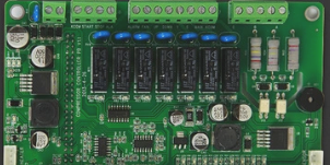
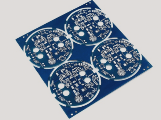
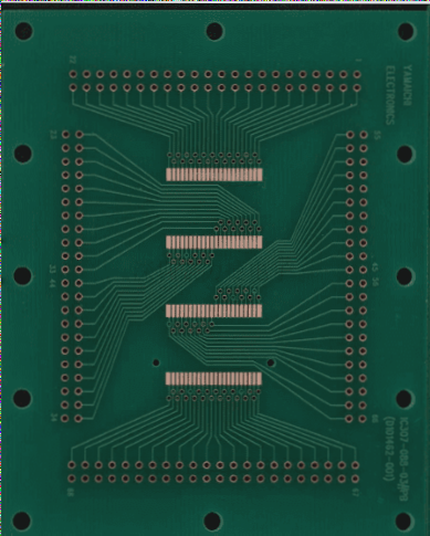
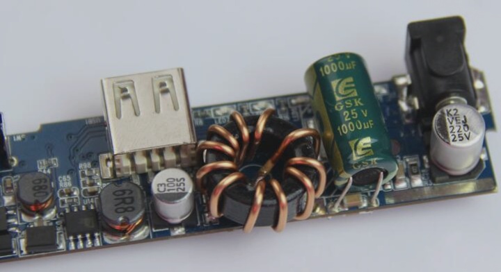
The manufacturing process for general electronic products consists of two main parts: PCBA and Box Build. Some factories focus solely on circuit board assembly (PCBA) and subsequently send the boards to another facility for finished product assembly (Box Build). Others handle the entire process from start to finish. The manufacturing process is as follows:
**SMT Manufacturing Process:**
1. **PCB Loading:** Typically, the PCB is manually placed into the Magazine Rack (material rack) to enable automatic feeding during production.
2. **Glue Dispensing:** Initially used in early circuit boards requiring the “wave soldering” process, glue is applied beneath the electronic components. This ensures the components adhere to the circuit board after baking, preventing them from falling into the tin furnace during wave soldering.
3. **Solder Paste Printing or Glue Printing (MPM):** This process involves applying solder paste to the circuit board using a stencil. The solder paste acts as a bridge between the PCB and electronic components.
**Choosing Solder Paste:**
This section introduces fundamental knowledge regarding solder paste selection.

4. **Solder Paste Inspection**: Some factories may not implement a solder paste inspection process, which primarily aims to identify issues with solder paste printing before component placement. This includes checking for misalignment and ensuring the appropriate amount of solder paste is applied, allowing for the correction of any printing issues that could lead to poor soldering.
5. **Pick & Place**:
– Fast machine: Small components (e.g., resistors, capacitors, inductors) (small chip).
– Slow-speed machine: General-purpose machine for larger components (e.g., ICs, connectors).
– Special-shaped machine: Primarily designed for clamping; can also place parts from trays.
– Hand placement: If machines are unable to place components, manual placement is done at the end (not recommended).
**SMT Related Articles**:
– Pallet packaging tape and reel packaging
– Comparison of the advantages and disadvantages of Tray and Tape-on-reel packaging in SMT
– [Technology] Red Dye Penetration Test
– [SMT] Matte tin vs. Bright tin
6. **Reflow**: See another article on Reflow Profile.
7. **Auto Optical Inspector (AOI)**: This system optically checks for incorrect, missing, misaligned parts, poor solder joints, insufficient solder, solder shorts, and solder balls. Detecting voids and false solder connections is challenging.
8. **Hand Soldering Parts**: Some electronic components cannot be processed with current SMT machines. For small quantities, hand soldering is used; for larger amounts, wave soldering is considered.
9. **Receiving and Visual Inspection of Appearance**: Upon receipt, the PCB automatically enters the Magazine Rack (material rack) to prevent collisions between electronic components.
**PCBA Test**
10. **PCBA De-paneling**:
– V-Cut: Folded edge.
– Router: Similar to a bed wash, removing board edges.
11. **PCBA Test**:
– MDA/ICT
– Function Test
Steps 10 and 11 can be interchanged based on process requirements.
12. **Finished Product Assembly (Box Build)**
13. **Burn-in Test**: Discussion on the pros and cons of product aging tests.
14. **Final Test**
15. **Ship to Stock**
**SMT Manufacturing Process:**
1. **PCB Loading:** Typically, the PCB is manually placed into the Magazine Rack (material rack) to enable automatic feeding during production.
2. **Glue Dispensing:** Initially used in early circuit boards requiring the “wave soldering” process, glue is applied beneath the electronic components. This ensures the components adhere to the circuit board after baking, preventing them from falling into the tin furnace during wave soldering.
3. **Solder Paste Printing or Glue Printing (MPM):** This process involves applying solder paste to the circuit board using a stencil. The solder paste acts as a bridge between the PCB and electronic components.
**Choosing Solder Paste:**
This section introduces fundamental knowledge regarding solder paste selection.

4. **Solder Paste Inspection**: Some factories may not implement a solder paste inspection process, which primarily aims to identify issues with solder paste printing before component placement. This includes checking for misalignment and ensuring the appropriate amount of solder paste is applied, allowing for the correction of any printing issues that could lead to poor soldering.
5. **Pick & Place**:
– Fast machine: Small components (e.g., resistors, capacitors, inductors) (small chip).
– Slow-speed machine: General-purpose machine for larger components (e.g., ICs, connectors).
– Special-shaped machine: Primarily designed for clamping; can also place parts from trays.
– Hand placement: If machines are unable to place components, manual placement is done at the end (not recommended).
**SMT Related Articles**:
– Pallet packaging tape and reel packaging
– Comparison of the advantages and disadvantages of Tray and Tape-on-reel packaging in SMT
– [Technology] Red Dye Penetration Test
– [SMT] Matte tin vs. Bright tin
6. **Reflow**: See another article on Reflow Profile.
7. **Auto Optical Inspector (AOI)**: This system optically checks for incorrect, missing, misaligned parts, poor solder joints, insufficient solder, solder shorts, and solder balls. Detecting voids and false solder connections is challenging.
8. **Hand Soldering Parts**: Some electronic components cannot be processed with current SMT machines. For small quantities, hand soldering is used; for larger amounts, wave soldering is considered.
9. **Receiving and Visual Inspection of Appearance**: Upon receipt, the PCB automatically enters the Magazine Rack (material rack) to prevent collisions between electronic components.
**PCBA Test**
10. **PCBA De-paneling**:
– V-Cut: Folded edge.
– Router: Similar to a bed wash, removing board edges.
11. **PCBA Test**:
– MDA/ICT
– Function Test
Steps 10 and 11 can be interchanged based on process requirements.
12. **Finished Product Assembly (Box Build)**
13. **Burn-in Test**: Discussion on the pros and cons of product aging tests.
14. **Final Test**
15. **Ship to Stock**


