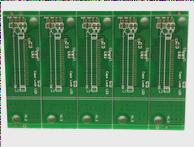
The PCB profiling process involves cutting the production panel into specific sizes and shapes according to the customer’s design specifications. To streamline the PCB assembly process, the boards can be profiled either as individual boards or in panelized forms, depending on their size and quantity. PCB panelization helps improve soldering efficiency during assembly. For irregularly shaped boards, panelization also maximizes the use of board area, thereby reducing material waste and manufacturing costs. There are two main methods for profiling rigid PCBs: Tab Routing and V-Scoring. The choice of method depends on the panelization technique, board shape, and other factors.
Tab Routing
Tab routing is a process where a milling machine is used to cut the specified panel patterns according to the outline file, achieving high dimensional accuracy and a smooth surface finish. During the routing process, registration holes are drilled in the pad of the milling machine, and the board is secured in place with pins. The routing process follows the outline data, and multiple boards can be processed simultaneously. After routing, a cleaning operation is required to remove any dust, debris, or residues left on the surface, in holes, or in V-shaped grooves. Once cleaned and dried, the board is sent for quality control inspection.
V-Scoring
V-scoring is another method for profiling boards, where a V-shaped groove is cut along both sides of the circuit board that needs to be separated, using a V-scoring machine. The depth of the groove is typically about one-third of the board’s thickness. This method allows easy separation of the panels after assembly while keeping the individual boards intact. V-scoring is a cost-effective method for PCB panelization, reducing material and fabrication costs. However, it is mainly suitable for square panels and cannot process multiple panels at the same time.
If you have any questions about PCBs or PCBA, please feel free to contact us at info@wellcircuits.com.


