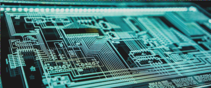
Impact of PCB Quality on Soldering Processes
Reflow Soldering Process
- Insufficient pad plating thickness can lead to poor soldering quality.
- Dirty pad surfaces hinder proper wetting of the tin layer.
- Offset wet film on pads can cause soldering issues.
- Incomplete pads may result in weak component soldering.
- Unclean BGA pad development can lead to improper tin adherence.
- Protruding BGA plug holes may cause detachment of components.
- Oversized solder mask around BGAs risks short-circuiting.
- Incorrect spacing between holes and patterns can cause misalignment.
- Breakage of green bridges between IC pads can result in short circuits.
- Protruding via plug holes near ICs hinder proper mounting.
- Breakage of stamp holes between cells affects solder paste printing.
- Incorrectly drilled identification light spots can cause part misplacement.
- Secondary drilling of NPTH holes leads to misalignment of solder paste.
- Flat, matte light spots next to ICs or BGAs aid machine recognition.
- Avoid nickel-gold reflow on mobile phone boards to maintain signal quality.
Wave Soldering Process
- Presence of green oil in component holes can impact soldering quality.
- Inadequate hole wall plating thickness may lead to poor soldering.
- Excessive roughness of hole walls can affect tinning and solder joint quality.
- Moisture in holes can cause virtual welding or air bubbles during soldering.
- Insufficient pad size can result in poor soldering and potential damage.
- Dirty hole interiors can hinder proper tinning and soldering.
- Inadequate hole aperture size may prevent proper component insertion.
- Misaligned positioning holes can impede component insertion and soldering.
- Excessive board warpage affects overall soldering quality.
Ensuring high-quality PCBs is crucial for successful soldering processes and reliable electronic assemblies.
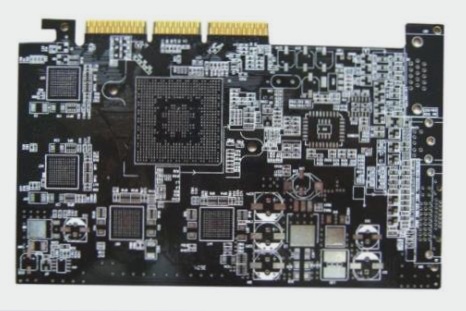
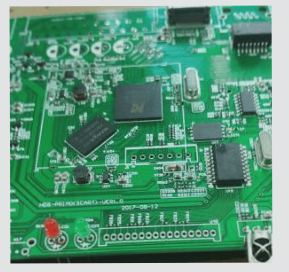
The Impact of PCB Quality on Hybrid Assembly
Quality PCB boards play a crucial role in hybrid assembly processes, especially when dealing with a mix of surface-mounted and through-hole components. It is essential to carefully manage the soldering surface properties, such as tin thickness and surface flatness, to guarantee the secure attachment of components throughout the reflow, adhesive curing, and wave soldering phases. In particular, it is vital to steer clear of polytin on tin-sprayed boards to prevent component detachment during wave soldering.
Latest Insights:
- Recent studies suggest that using advanced solder mask materials can further enhance the overall quality and reliability of PCBs.
- Implementing automated optical inspection (AOI) systems can significantly improve the detection of defects in PCB assemblies, leading to higher manufacturing yields.